LabAdviser/Technology Research/Nanofabrication of Inductive Components for Integrated Power Supply On Chip/Air-core Inductor
Through-silicon Etching
| Step | Description | LabAdviser link | |
|---|---|---|---|
| 1.1 | Si wafer | Start with a 100 mm Si<100> wafer that is double side polished with a thickness varies from 280 µm to 500 µm. | Wafer information, types of avaliable wafers are listed. |
| 1.2 | Al2O3 ALD deposition | Grow a 50nm aluminum oxide as hard mask for DRIE by thermal ALD (ALD1) | ALD Picosun R200. |
| 1.3 | Lithography | The wafer has to be RCA cleaned, before entering an oxidation furnace. | UV lithography, 1.5-µm-thick Mir 701 positive resist is used. Parameters (dose: 210 mW/cm2, hardbake: 150 oC@30min) |
| 1.4 | Al2O3 Wet Etching | Al2O3 is etched to open the TSVs prior to through-silicon DRIE. | UV lithography. Etch ALD Al2O3 in 5% BHF using a beaker setup. The etch rate is approximately 50 nm/min |
| 1.5 | Through-silicon DRIE | Si wafer is etched through to create hollow TSVs by DRIE. Wafer is firstly glued to a carrier wafer using Crystal Bond. The masking materials are 1.5µm photoresist and 50nm Al2O3. Etching will stop at an Al2O3 layer on the other side. | DRIE Process A is used. |
| 1.6 | Cleaning | The masking materials are removed and wafer is then cleaned. | The DRIE-etched Si wafer with TSVs is cleaned with the following procedures: crystal bond removal, O2 plama clean (Plasma Asher 1), Al2O3 removal using BHF, Piranha |
| 1.7 | Insulation layer deposition: Al2O3 and SiO2 | ALD Al2O3 (Al2O3T recipe) and PECVD SiO2 are deposited. | ALD Picosun R200 and PECVD3 |
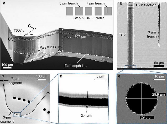
Etching profile after DRIE (step 5). (a) SEM micrograph of a cleaved Si wafer showing the etching profile at the Si fixture. Enclosed in the fixture, there are three TSVs which have been etched through. As depicted in the inset taken from the process ow, the fixture trenches are etched with shallower depths of 233 um and 307 um for 3 um and 7 um fixture trenches, respectively. (b) Cross-sectional SEM micrograph (C-C direction) of the TSV and 3- um trench. This sample was cut with a diamond blade. (c) A top view (frontside) of the etching profile at a fixture trench, (d) A top view of the etching profile zoomed at the 3-um segment of the fixture trench, (d) A top view (backside) of the etching profile of a TSV.
Copper Electroplating
| Step | Description | LabAdviser link | |
|---|---|---|---|
| 2.1 | Seed layer deposition | 10nm Ti and 100 nm Au are deposited by e-beam evaporation on one side of the wafer. The alignment marks are covered by using Kapton tape. | Wordentec |
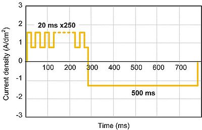
| 2.2 | Cu Electroplating: 1st Layer Deposition | Electroplate a 30 µm Cu on wafer frontside, on which the fixture trenches are located. The goal is to close the 30-µm TSVs and the fixture trenches, thus providing an electrical path for later bottom-up TSV filling step. The preparation procedure is as follows: wafer is cleaned by Acetone and IPA, wafer is degassed using a desiccator, wafer is mounted on a plating holder while being immersed in DI wafer to avoid air trapped in the TSVs. Reversed pulsed current is used to achieve good uniformity (< 5%) and to effectively close the TSVs. | The process was done at IPU. |
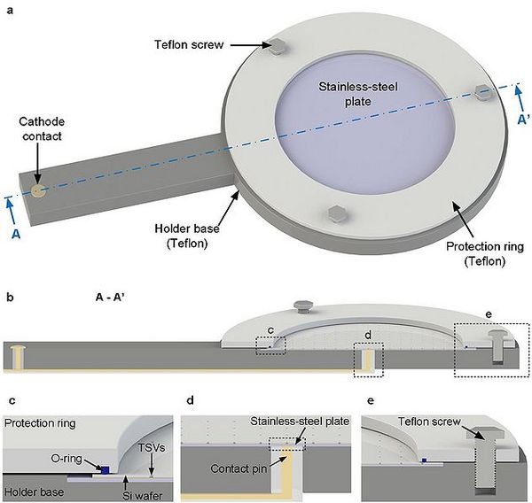
| 2.3 | Cu Electroplating: 2nd Bottom-up TSV Filling | The wafer is then placed up-side-down on a special wafer holder. The design of the holder is shown below. The preparation procedure is as follows: Acetone and IPA clean, desiccator degassing, mounting on the holder under DI water. A low current-density DC current is applied. This step was done overnight as to fill a 300-µm-tall, 30-µm-diameter TSVs takes 16 hours. | The process was done at IPU. |
| 2.4 | Cu Electroplating: 3rd Layer Deposition | The wafer is then brought back to Cleanroom, undergoing cleaning steps followed by a deposition of seed layer (10nm Ti and 100 nm Au). The electroplating step is repeated as same as Step 2.2 without the need of a degassing step. | The process was done at IPU. |
| 2.5 | Lithography on spray-coated resist | Spray coating is used to pattern resist masks on both wafer sides prior to wet etching of Cu. AZ 4562 is used. The target thickness is 3 µm achieved by the following coating parameters (flow: 2000 µl/min, substrate temperature: 29 oC, meander path: 100 mm/s, 5mm between spraying lines). The specific parameters are: Step 10.1: HMDS Primer: HMDS oven (model 310TA-E, Pump-down 2 min; Nitrogen purge 3.5 min;
Heat-up 10 min; Pump-down to 3 mBar; HMDS prime 5 min; Chamber exhaust 3 min; Nitrogen purge, 3.5 min). Step 10.2: Spray coating and photolithography (2500 µl/min) AZ 4562, exposure (multiple exposure 20s x 4 x 7 mJ/cm2), development (1:5 AZ 351B, 300s, 22 oC). |
SprayCoater |
| 2.6 | Cu Wet Etching | Wet etching of Cu to define inductor windings. APS 100 Cu Etchant is used. The etch rate is approximately 3 µm/min. Both sides of the wafers are etched at the same time. It is noticed that this wet etching step is not uniform on devices across a 4-inch wafer, therefore, it is stopped when the first patterns are completely etched. Then, the etching continues on each side of the wafer with constant inspections under optical microscope. The etch rate is approximately
0.5 µm/min at room temperature. A photoresist mask (AZ 4562, Microchem., USA) is used as an etch mask. Etching setup in a beaker: (the wafer facing down with a stirrer spinning for agitation). The etchant is APS 100 (Transence, USA). |
This was done in a beaker setup. |
| 2.7 | Seed layer removal. | After etching, the Ti/Au seed layers are removed by using a commercial gold etchant
Entreat 100 (Engtech Scandinavia A/S) with a concentration of 43 g/L and 5% HF, respectively. Cleaning: Ultrasonic cleaning + trixton, rinsing with DI water, and spin drying. |
The process was done at IPU. |
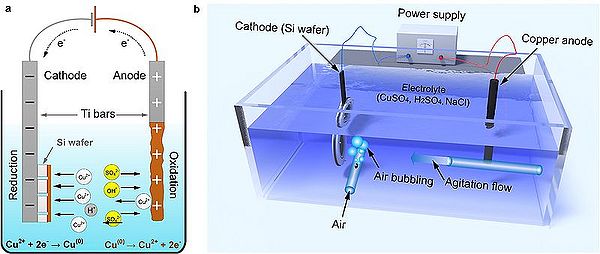
The setup of the Cu plating bath. (a) Working principle of Cu electroplating using SO4-based solution. The sample to be plated is connected to the negative cathode while a Cu plate is placed at the positive anode. The electroplating process is described as reduction and oxidation reactions occur at cathode and anode, respectively. As the current is applied, the oxidation reaction occurs at the anode creating Cu2+ ions which are then driven to deposit on the cathode. (b) Schematic representation of a 25 L plating bath. Air bubbling agitation is used. The electrolyte consists of 140 g/L CuSO4, 140 g/L H2SO4 and 66 mg/L NaCl.
Pulsed current waveform for Step 2.2: TSV closing.
A final design of the wafer holder for TSV-filling process (step 8). (a) A 3D design of the holder with two parts: a holder based, a protection ring, and a 200-um-thick stainless-steel plate. The protection ring is attached to the holder base by three Te on screws. (b) A crosssectional view (A-A' direction) of the holder with three zoomed views: (c) O-ring attached to the protection ring for protecting the edge of the Si wafer with closed TSVs. (d) An electrical connection between the contact pin and the stainless-steel plate. (e) A Te on screw for fastening the holder.
Cu electroplating and wet-etching results. (a) top-view SEM micrograph after the 1st plating of 30-µm-thick Cu layer (step 7). All TSVs and the fixture trench are closed which provides the electrical path for bottom-up TSV filling. The transparent red line illustrates the µxture trenches which have been closed. Copper filled 35 µm into the TSVs as shown in the subµgure. (b) void-free Cu-µlled TSV after 13.5 hours of plating at 0.5 A/dm2 (step 8). (c) wet-etched toroidal Cu windings (step 9). The red lines are isotropic wet-etch compensations on the photolithography mask design. Winding pitch (GW) increased from the designed 40 to 94.3 µm due to the lateral undercut.
Preliminary results of a mold-based electroplating for denser inductor windings. (a) A 50-µm-thick AZ 125 nXT mold for electroplating of the top Cu layer. (b) 45-µm-thick top Cu layer deposited in the resist mold. A winding gap of 40 µm is demonstrated.
3. Spray Coating and Silicon-Core Removal
| Step | Description | LabAdviser link | |
|---|---|---|---|
| 2.1 | Aluminum oxide deposition | Grow a 50nm aluminum oxide as hard mask for DRIE by thermal ALD (ALD1) | ALD Picosun R200. |
| 2.2 | Spray coating of photoresist | Two-step recipe (2000 µl/min x2). | SprayCoater |
| 2.3 | Lithography of spray-coated resist | Soft baking (12 hours storing in N2 cabinet, 60 oC baking in convection oven), exposure (multiple exposure 20s x 8 x 7 mJ/cm2), development (1:5 AZ 351B, 300s, 22 oC) | Ovens |
| 2.4 | Aluminum oxide etching using BHF | Etch rate is approximately 50nm/min | The process was done in a beaker setup. |
| 2.5 | ICP Isotropic etching of Si core (Hoa_ISO1 recipe) | The specific parameters are: Gas flow (sccm) SF6 230, O2 23; Cycle time (secs) 3.0; Pressure (mtorr) 10; Coil Power (W) 2800; Platen Power (W) 3; Temperature: 20 oC, APC mode manual, APC setting: 87.7%. Etch rate 10 µm/min, etch time 80 min. | Advanced Silicon Etch |
| 2.6 | Clean, Dry, and dicing | Resist stripping using O2 Plasma: 1000 W, 400 sccm O2, 70 sccm N2, 30 min.
Al2O3 Stripping: Al2O3 removing by BHF, DI water clean. Dry clean by nitrogen gas. Dicing: is done by a laser microSTRUCT (3D-Micromac). 1024 nm laser is used. The cutting patterns has 3 parallel lines (30 m pitch) with 50 times repetition to cut through a 280 µm-thick Si wafer. |
This was done in a beaker setup. |
Spray Coating Optimization
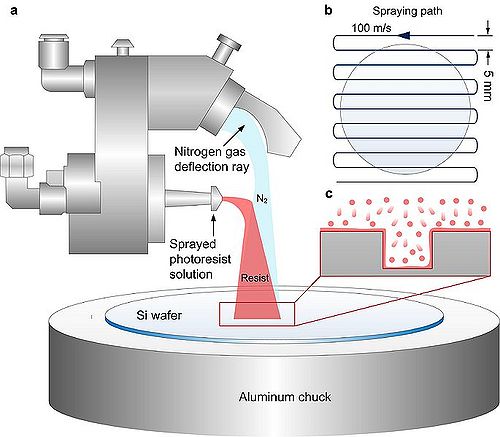
Figure 1 shows the spray coater setup. The wafer is placed on an aluminum chuck at 28 degree Celcius. The spraying path follows a meander path as shown in Fig. 1b. The distance between two spraying lines is 5 mm. The parameters of spraying recipe is presented in Table I.
Fig.1. Spray coating Setup.
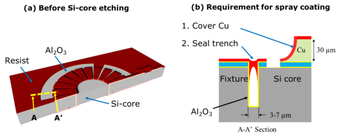
Fig.2. Spray coating requirements.
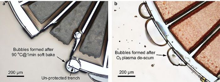
Air Bubbles are formed after a quick 90 oC soft-baking step for 1 min (a). (b) a 1-min de-scum step using O2 plasma. The sprayed resist that has filled in the trench expands and forms bubbles at the vacuum of 1.0 mbar during the O2 plasma process. The bubbles leave some unprotected area on the fixture trench thus resulting in the erosion of the Si support and fixture trench in the later Si-core etch step.
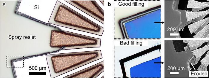
Good and bad filling and the corresponding results in the Si-core etch step. (a) Optical micrograph top-view of patterned spray-coated resist at Si fixture (step 12). Good and bad fixture trench resist sealing are shown in the top and bottom insets. (b) Si core etching results corresponding to good and bad sealing.
Results
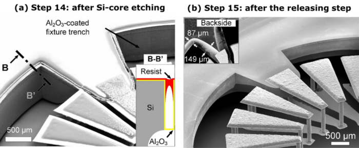
The results after Si-core isotropic etching. (a) A hollow Al2O3 stopping barrier on fixture trench (B-B' cross section is depicted in the inset) and Al2O3/SiO2 membrane at bottom remained after isotropic ICP Si etching. (b) A well-defined Si-fixture on the final inductor after the BHF releasing step, and the fixture backside is shown in the inset.

