Specific Process Knowledge/Thin film deposition/Temescal/Acceptance Test
Feedback to this page: click here
Temescal acceptance test results

In the acceptance test, we tested the vacuum performance, the ion source, and the uniformity of the deposited metal films.
The uniformity of the ion beam etch was tested on Si wafers with SiO2 coating of a known thickness.
For metal films, the thickness and for Ti/Ni the sheet resistance uniformity were measured.
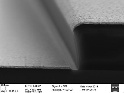
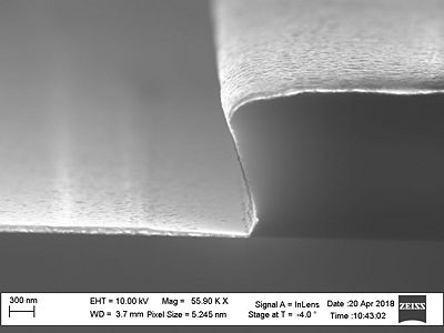
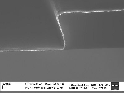
Side wall coverage was evaluated in SEM for Ti/Au films deposited at normal incidence (what most users require, which gives no side-wall deposition) and with various degrees of tilt.
Full acceptance test report here
Thickness uniformity
The thickness uniformity is good both across a single wafer, from wafer to wafer within a batch of 4 wafers and from batch to batch comparing up to 5 batches. This is ensured by the Hula sample holder, which rotates each individual wafer holder around its axis as well as all four wafer holders around the central axis.
We saw less than 3 % variation across a 6" wafer and comparable or lower variation wafer to wafer and batch to batch.
The thickness uniformity was not tested for the 8" sample holder nor for the tilted sample holder.
We cannot guarantee that the batch-to-batch thickness reproducibility will always be below 3 % as there may be more drift over longer times. We check the thickness of a Ti/Au deposition every month and ensure that it is within 10 % of the expected value and so far, within in the first half year of using the instrument, the variation has been much less than 10 %.
Sheet resistance uniformity
The sheet resistance varied less than 2 % across a single 6" Ti/Ni coated wafer and less than 1 % from wafer to wafer comparing a total of 4 wafers made in two different batches.
Note that thickness variation will lead to variation in the sheet resistance, so accurate thickness is important for reproducible sheet resistance values.
Ion source
We achieved an etch rate of up to 1 nm/min for SiO2. The etch rate is strongest in the center, about 15-20% higher than at the edges of a 6" wafer.
The reproducibility was quite good with less than 3% variation wafer-to-wafer within a batch and less than 10 % variation between the two identical batches.
Vacuum performance
Pumpdown of the load lock from atmosphere took 15 minutes to below 10-6 Torr, which is the process pressure. Note that this was with a brand new vacuum chamber. The pumping time is slower the more material is deposited inside the machine, as the layers can trap moisture and other gases.
A pumpdown of the whole system took about 1.5 hours to below 10-6 Torr.
More results in the full report.
Side wall deposition on tilted samples
The tilted sample holder was tested with 10 nm Ti/100 nm Au deposition at approx. 27 °, 45 °, and 53 ° to the normal (53 ° is the max tilt variation for a 6" sample holder - we now have a smaller 2" sample holder that can tilt all the way to perpendicular to the evaporation source).
As expected, the side wall deposition was thicker for 53 ° tilt than for 17 ° tilt.


