Specific Process Knowledge/Etch/Etching of Silicon Oxide/SiO2 etch using AOE
Feedback to this page: click here
What masking material should I choose when etching SiO2/glass in the AOE?
Photoresist mask - not too deep etches
Etching SiO2 with resist as masking material is the prefered masking material for many purposes. The main reason for using photo resist as masking material is that it is easy and fast to make and easy to remove afterwards. The selectivity of resist to SiO2 is in the range of 3-4.
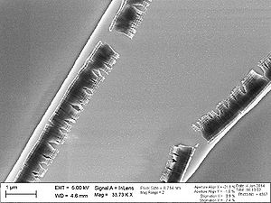
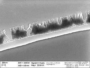
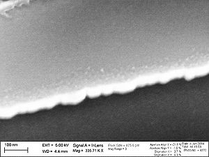
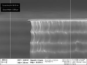
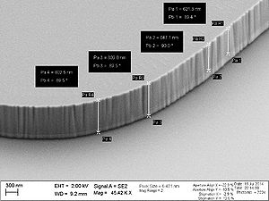
The main draw back when using photoresist as masking material is heating of the substrate during the etch. SiO2 is a hard material to etch and therefore needs a high DC bias to allow the ion bombardment to be enegetic enough to etch the SiO2. This ion bombardment heats up the surface and even when cooling the platen to zero degrees Celcius the resist mask can exceed 100 degrees Celcius. Combined with the fact that the plasma UV hardens the surface of the resist this can create crumpled resist surface and perforated egdes, see images here. Etching a few microns down in the SiO2 normally does not heat up the resist too much but when etching deeper like 5-10µm there is a large change for getting problems with overheating the resist.
Si/P-Si mask - deeper etches
P-Si is a good masking layer for deeper etches. The selectivity to SiO2 is measured to be better than 1:15. The P-Si on the back side seems to prevent declamping of a APOX substrate during a deep etch on a high load wafer (e.g. 50% load), contrary to using photo resist mask on the APOX substrate. The wafer bow is created when removing part of the top oxide layer due to stress in the oxide layers.
Draw backs: the recipe we have now is giving a high line width reduction (1µm when etching 7.5µm down). Take a look at some recipes and results
Al mask - deeper etches - more redeposition
Al is allowed as masking material but we do not advise it. It can however be useful under some curcumstances. It is expected to have a high selectivity to SiO2 greater than 50.
Draw back: The draw back is that Al does not form any volatile products with the Flour gasses. This means that any Al sputtered of has the chance of getting redeposited on the surface.
Cr mask - deeper etches/high aspect ratio etches where the other materials cannot be used
Cr works well as masking material but due to cross contamination issues we prefer to avoid Cr in the machine. Cr does in contrary to Al form some volatile components with the flour gasses and therefore redeposition problems are not so severe. We do allow Cr as masking material when the other masking materials cannot be used.
So fare it has been found useful for etching nanostructures in quartz substrates.
Etching of micro structures in Silicon Oxide with resist as masking material
| Quality Controle (QC) for AOE | ||||||||||||||||||||||||||
|
Standard silicon oxide etch using resist as masking material
The standard recipe for etching SiO2 with resist mask
Slow etch of SiO2 with resist as masking material - e.g. for use with carrier
Etching with CSAR resist as masking material
Information given by Alberto Cagliani February 2015
Using the standard oxide recipe (SiO2_res) for 1 min the CSAR looked burned and could not be removed by CSAR stripper (AR600-71). Using the following settings the resist did not looked burned and could be removed by CSAR stripper:
| Parameter | Recipe name: |
|---|---|
| Coil Power [W] | 450 |
| Platen Power [W] | 80 |
| Platen temperature [oC] | 0 |
| He flow [sccm] | 174 |
| C4F8 flow [sccm] | 5 |
| H2 flow [sccm] | 4 |
| Pressure [mTorr] | 4 |
| Typical results | Negative Resist mask DANCHIP result |
|---|---|
| Etch rate of thermal oxide | ~105nm/min (<5% etch load) |
| Selectivity to CSAR [:1] | ~2 |
| Profile [o] | not measured |
| Images | none |
| Comments | CSAR did not burn and could be removed by AR600-71 |
Etching of micro structures in Silicon Oxide with PolySi as masking material
The choice of recipe depends on your preferences. Some different etch rate recipes are given here. You can choose between getting
High etch rate recipe
| Parameter | Recipe name: SiO2_psi (SiO2 etch with pSi mask) |
|---|---|
| Coil Power [W] | 1300 |
| Platen Power [W] | 500 |
| Platen temperature [oC] | 60 |
| He flow [sccm] | 300 |
| C4F8 flow [sccm] | 18 |
| H2 flow [sccm] | 0 |
| Pressure [mTorr] | 4 |
| Typical results | PolySi mask - tested by Yunhong Ding @fotonik | PolySi mask - tested Feb. 2012 by bge@danchip |
|---|---|---|
| Etch rate | ~0.55 µm/min | 0.50 µm/min |
| Selectivity | 1:~10 | 1:17 |
| SiO2 etch uniformity | not tested | ±4.5% over a 100mm wafer |
| Profile [o] | not tested | see images |
| Images | . | See here |
| Comments | . | Line width reduction is about 2.5µm when etching 12.5µm down. See the images to get more info on this |
Low line width reduction recipe
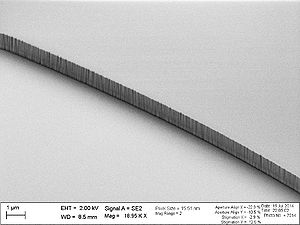
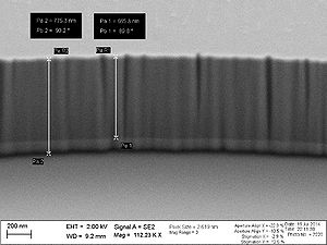
It is difficult to get very low line width reduction using P-Si as masiking material. This is due to the fact that the etch gas C4F8 that is used to etch SiO2 also etches Si very well. The best result so fare is given here:
| Parameter | Poly Si mask |
|---|---|
| Coil Power [W] | 1100 |
| Platen Power [W] | 170 |
| Platen temperature [oC] | 50 |
| He flow [sccm] | 450 |
| C4F8 flow [sccm] | 12 |
| H2 flow [sccm] | 0 |
| Pressure [mTorr] | 6 |
| Spacer settings [mm] | 100 |
| Typical results | PolySi mask - tested spring. 2012 by bge@danchip |
|---|---|
| Etch rate | ~0.25 µm/min |
| Selectivity | 1:12 |
| SiO2 etch uniformity | ±1.1% over a 100mm wafer |
| Profile [o] | see images |
| Images | See here |
| Comments | Line width reduction is about 1µm when etching 7.5µm down. See the images to get more info on this |
Good wafer uniformity recipe
This recipe has not been optimized to get as uniformity as possible but was just the one with the lowest non-uniformity among the recipes I have tested.
| Parameter | Poly Si mask |
|---|---|
| Coil Power [W] | 1300 |
| Platen Power [W] | 350 |
| Platen temperature [oC] | 60 |
| He flow [sccm] | 450 |
| C4F8 flow [sccm] | 18 |
| H2 flow [sccm] | 7 |
| Pressure [mTorr] | 8 |
| Spacer settings [mm] | 0 |
| Typical results | PolySi mask - tested spring. 2012 by bge@danchip |
|---|---|
| Etch rate | ~0.40 µm/min |
| Selectivity | 1:10 |
| SiO2 etch uniformity (±(max-min/2*avg) | ±0.54% over a 100mm wafer |
| Profile [o] | see images |
| Images | See here |
| Comments | Line width reduction is about 3µm when etching 14µm down. See the images to get more info on this |
High selectivity to Si-mask recipe
This recipe has not been optimize to get as good selectivity as possible but was just the one with the highest selectivity among the recipes I have tested.
| Parameter | Poly Si mask |
|---|---|
| Coil Power [W] | 1300 |
| Platen Power [W] | 350 |
| Platen temperature [oC] | 20 |
| He flow [sccm] | 450 |
| CF flow [sccm] | 18 |
| H flow [sccm] | 7 |
| Pressure [mTorr] | 8 |
| Spacer settings [mm] | 0 |
| Typical results | PolySi mask - tested spring. 2012 by bge@danchip |
|---|---|
| Etch rate | ~0.43 µm/min |
| Selectivity | 1:24 |
| SiO2 etch uniformity | ±2.2% over a 100mm wafer |
| Profile [o] | see images |
| Images | See here |
| Comments | Line width reduction is about 3µm when etching 13µm down. See the images to get more info on this |
Etching of micro structures in Aluminum oxide
by Fredrik Stöhr
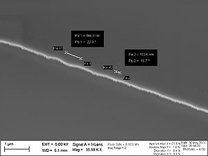
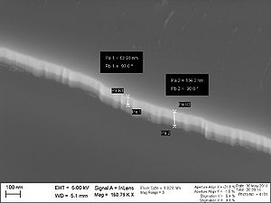
Aluminum oxide (Al2O3, Alumina) can be etched with the standard recipe for silicon oxide etching. The parameters including the chuck temperature are identical to the recipe described above: SiO2_res. The etch is probably very physical and gives redeposition, so please consider using a Cl2 etch on the ICP metal instead (BGHE 2015-04-17)
General Description
- Process date: Summer 2014
- Aluminum Oxide with a thickness of 50 nm has been deposited by atomic layer deposition using the respective standard recipe.
- Substrates: Blank 525 µm Silicon wafers or Silicon wafers with thermally grown Silicon Oxide prior to Alumina deposition.
- Mask: [XOP8] AZ5214E 1.5 µm thick (HMDS pretreatment, 6-inch aligner 3 sec exposure, 60 sec development).
- Etch Load (Total Exposed SiO2): ~ 5 %
- Post process: O2 Plasma Ashing 10 min
Limitations using the AOE
Wafer bow
There is a limit to how much the wafer can bow and still be clamped on the chuck. The limit can maybe vary a little over time and may also depend on the material on the backside of the substrate. On a 100mm Si wafer with SiO2 on the backside (<10µm) we expect the limit to be around 50µm bow (when the back side surface is convex).
A bow will be created when etching the top oxide layer on a wafer with oxide on both sides. For a larger etch load the bow will be more severe for a specific etch depth when for a smaller etch load. I have been able to etch much deeper in SiO2 with a P-Si mask than with a photo resist mask on a wafer with 50% load. When using photoresist the wafer stopped clamping during the etch after just a few µm. With P-Si I could etch 15µm without problems. I expect this to be due to a combination of P-Si on the back side clamping much better and P-Si on the back side helping to reduce the bow.
Transparent wafers
Transparent wafers are a challange for two reasons. 1. In the load lock the LASER detection system that is used to detect the wafer during mapping cannot detect a completely transparent wafer. 2. A transparent wafer is either quartz or fused silicon. These materials are very difficult to clamp electrostatically and will therefore not be able to pass the He leak up test succesfully.
- The first issue may be overcome by using a non-transparent masking material or adding a non-transparent material on the back side of the wafer (could be aluminium).
- The second issue may be overcome by reducing the He back side pressure or reducing the He back side cooling completely. Another way to solve it is to either bond the transparent wafer to a silicon wafer before transfering it into chamber or deposite a more conducting layer on the backside of the wafer. This could be aluminium but also 1-2µm P-Si may be enough.

