Specific Process Knowledge/Lithography/EBeamLithography/High resolution patterning with HSQ
- This work was done by Bingdong Chang and Xiaoli Zhu in 2016;
- This page was edited by Bingdong Chang 23 October 2017.
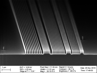
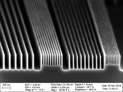
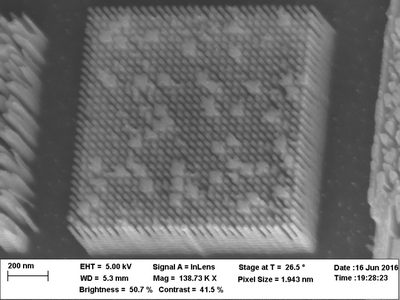
High resolution patterns (sub-10nm dots with 20nm pitch, sub-10nm lines with 50nm pitch) can be patterned with HSQ resist. Some SEM images are shown as below:
- SEM images of high resolution HSQ patterns
-
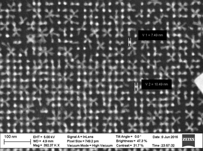 Dots with sub-10nm diameters
 -
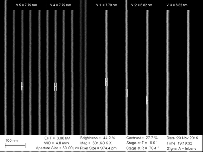 Lines with sub-10nm linewidths


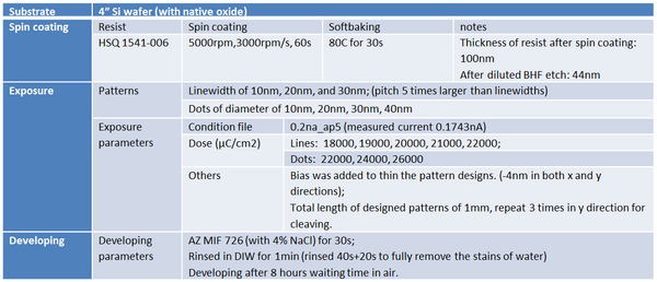
The details of the process is shown below in the table:
- Processing parameters for high resolution HSQ patterning
-

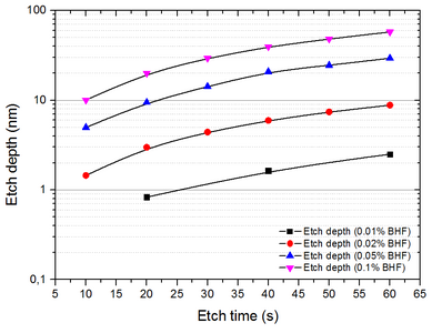
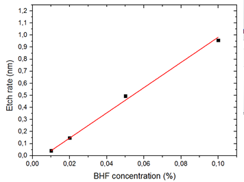
It should be noticed that to reduce the broadening of patterns caused by forward and backward scattered electrons, the HSQ resist was first thinned down to below 50nm using BHF before exposure. The etch rate of HSQ with different concentration of BHF is shown as below.
The details of the process is shown below in the table:
- Etch rate of HSQ (XR-1541 006) with BHF
-
-


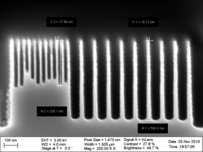
The patterns were successfully transferred into silicon by dry etching (with ASE, recipe Pxnano2)
- Etch rate of HSQ (XR-1541 006) with BHF
-
-
-
-


Notice that roughness could be generated during etch by redeposition of HSQ hard mask. For more details, please contact Bingdong Chang (bincha@dtu.dk).