LabAdviser/314/Microscopy 314-307/SEM/Nova
Feedback to this page: click here
The FEI Nova 600 NanoSEM
The FEI Nova 600 NanoSEM Scanning Electron Microscope is a very versatile characterization instrument that produces enlarged images of a variety of specimens, achieving magnifications of over 500.000 times providing ultra high resolution imaging. At the time being this microscope is mainly designated for microstructural characterization using electron backscatter diffraction (EBSD) , Energy-dispersive X-ray spectroscopy (EDS) and forward scatter electron imaging by detectors recently bought from Bruker.
Who may operate the FEI SEM
Currently, Dr. Alice Bastos Fanta is co-ordinating all the activities that take place on FEI Nova 600 NanoSEM. So she must be informed about the planned activities before hand in the bi-weekly meetings which are held at DTU-Cen. She makes the bookings in agreement with all the users. The rules of who may operate the FEI SEM and to what extent they may operate it are:
- Only users who have been trained and approved by DTU-Cen personnel may operate the instrument. Irregardless of their prior experience any new user with no official DTU-Cen training or approval cannot operate the instrument, not even under close supervision by experienced users.
- Users may only use the instrument to the extent they have been trained. This means that one should not try to operate the following options/capabilities without explicit training:
- Low vacuum
- EBSD capability
- EDX capability
- Backscatter detectors
How to operate the FEI Nova 600 NanoSEM
To find the basic instructions for operating the instrument, the reader is referred to the labmanager manual.
Processing guidelines on the FEI SEM
When one combines the 6 different detectors, 2 vacuum modes and 3 SEM modes with the traditional SEM parameters such as high voltage, working distance, spot sizes etc. it is clear that the FEI SEM has a huge number of different ways to be operated in. The number of ways that produce ultra high quality images is, however, limited. It is therefore crucial that the operators share their knowledge of how to obtain great images.
Steps to follow
There is no single general approach to taking good images on the FEI SEM. These points below are only guidelines.
What kind of images are needed
It is important to consider what kind of images are needed before you start. The different requirements/conditions could be some of the following:
- High resolution at high magnification (above 10.000x) images are wanted
- For conducting samples: Use TLD and mount the sample so that short WD's are possible.
- For non-conducting samples: Mount the Helix detector and use short (app. 5 mm) WD.
- Images of very thin (> 10 nm) metal films on low atom number materials
- Use the backscatter detectors
- Images with high resolution, large field of view and depth of focus are wanted
- The TLD and Helix detectors do not provide large field of view and depth of focus when operated in SEM mode II.
Detectors on the FEI SEM
The FEI SEM has 6 electron detectors and 1 photon (X-ray) detector.
| Tag | Name | Vacuum mode | Signal | SEM modes |
|---|---|---|---|---|
| ETD | Everhardt Thornley Detector | HiVac | SE, BSE (detector bias adjustable) | 1 and 3 |
| TLD | Through Lens Detector | HiVac | SE, BSE (detector bias adjustable) | 1, 2 and 3 |
| BSED | BackScatter Electron Detector | HiVac | BSE | 1, 2 and 3 |
| EBSD | Electron Backscatter Diffraction | HiVac | BSE | 1 and 3 |
| ARGUS | ARGUS(TM) | HiVac | BSE | 1 and 3 |
| LVD | Low Vacuum Detector | LoVac | SE + BSE | 1 and 3 |
| Helix | High resolution Low Vacuum detector | LoVac | SE | 1, 2 and 3 |
| GAD | Gaseous Analytical Detector | HiVac and Lovac | SE + BSE | 1, 2 and 3 |
| EDX | Energy Dispersive X-ray detector | HiVac and Lovac | X-ray photons | 2 and 3 |
Characterization Techniques
- Electron Backscatter diffraction
- Transmission Kikuchi diffraction
- Micro 4-point probe
Kleindiek micromanipulator
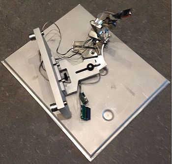
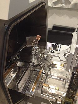
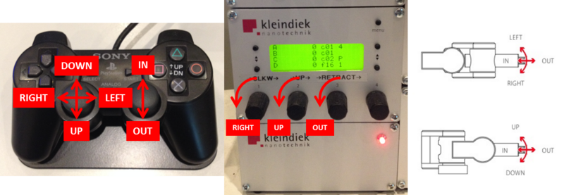
The Kleindiek Nanotechnik MM3A-EM is a plug and play micromanipulator for SEM/FIB applications, with a versatile range of modular plug-ins. The MM3A-EM can be used in most SEM/FIB instruments and offers fast setup and removal. The system consists of a base over which the micromanipulator arm is mounted (Figure 1). The base can be attached to the SEM front door by two exagonal head screws (Figure 2).The arm is connected to the external power supply through two plug-ins on a PCB board mounted on the SEM door.


