Specific Process Knowledge/Lithography/EBeamLithography/RaithElphy
Feedback to this page: click here
THIS PAGE IS UNDER CONSTRUCTION
Please contact William Tiddi for information and training on this equipment.
Manual
Technical Information
For an overview on the SEM imaging capabilities (which are relevant during patterning as well), see Specific_Process_Knowledge/Characterization/SEM:_Scanning_Electron_Microscopy
For information regarding patterning, see comparison table at Specific_Process_Knowledge/Lithography/EBeamLithography
Getting started
To request for an e-beam training session, contact e-beam@danchip.dtu.dk; a DTU Danchip personnel will hereafter provide a time slot. Users require at least 4 training sessions before being allowed full acccess to the machine. The first training will focus on file preparation and compilation alone.
It takes several months to get full authorization to the machine. Therefore, if you are either in a hurry, or a visiting researcher, or only require a few e-beam exposures to fulfill your project, let one of your authorized colleagues expose for you.
Before you request for a training on the machine, fulfill the following steps:
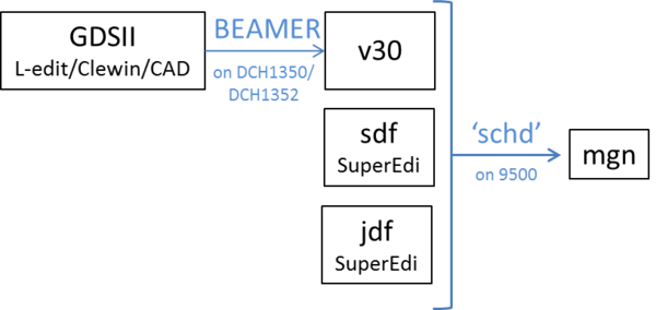
Prepare a v30-file:
- Prepare your pattern using a layout software (L-edit, CleWin, CAD) and export that to GDS format. Check your GDS-file by importing it in e.g. CleWin or L-edit. In order to reach the files from the computers inside the cleanroom it is recommended to either dropbox them or send them per email to yourself.
- Convert the GDS file to v30 using BEAMER; a manual for BEAMER software is found here
Create sdf and jdf-files:
- download SuperEdi,
- read the sdf and jdf-file manual found here,
- find templates of sdf and jdf files on the cleanroom drive in the folder E-beam sdf and jdf templates.
Gather Experience
- Assist a fully trained colleague of yours when she or he e-beam writes, gather as much knowledge about your e-beam run, i.e. which e-beam current, aperture and dose to use, which shot pitch (e.g. SHOT A,10).
- Study the logbook for the e-beam writer: sheet 1 gives you an overview of which condition files (currents and apertures) have been in use recently by which user on which type of resist. On sheet 2 in this logbook you can find a writing time estimation program.
- Study the manual for the machine, it can be found here
Prepare a process flow
- Describe your entire process in a process flow. The process flow should include all information such as type and thickness of resist, size and type of substrate, which processes are to be done before and after e-beam writing. Find process flow templates here. Attach your process flow to your request for training.
General Rules
For safety reasons, even fully trained users are only authorized to mount substrates into the e-beam cassettes, but not authorized to load the cassettes into the autoloader.
To use the e-beam writer, book the machine via LabManager, note the number and type of substrate as well as the condition file to be used in the 'Public Comment:' field in LabManager. Mount your substrate in the cassette and pre-align if necessary. Call for help from DTU Danchip staff to load your cassette into the robot loader (the autoloader).
After your exposure, fully trained users can unload their cassettes from the autoloader, unmount their substrates and re-load an empty cassette into the autoloader. If you are unable to unmount your substrates before another user requires the cassette, you must accept that either the next user or DTU Danchip personel unmount your substrates.
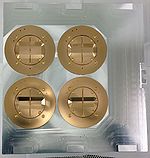
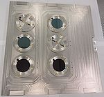
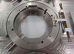
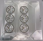
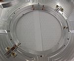
Cassettes
Some cassettes are made of Aluminum, others of Titanium. The thermal expansion coefficient of Ti is much lower than of Al; bear this in mind if you have crucial patterns to expose.
Keep an eye on the wafer orientation when you mount; the 2" aluminum cassette still have wafer orientation flat-up.
Design of global marks and chip marks
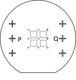
If you need to align an exposure to an existing pattern on a wafer you need wafer marks (or global marks) to align your exposure to. This requires global marks and chip marks on the wafer, optimization of gain settings of backscattered electron detector (ACGRG), and execution of subprograms that detects global marks and chip marks (SETWFR and CHIPAL). The subprograms are discussed in details in the manual.
Please note that manual alignment (using the SEM) is not allowed. You should use semi-automatic alignment only. In rare cases where semi-automatic alignment is impossible, you should remove the resist around the wafer marks before loading the wafer/chip into the machine.
1 Material:
Global marks or chip marks should be clearly visible in a 100keV SEM, i.e. preferably defined by Ti/Au or another 'heavy' metal, alternatively the wafer marks should be etched. In Si, etched mark should be around 1 µm deep in order to be detectable by the machine. Shallow etched (even 200 nm etched profiles) global marks or global marks in Si or marks defined by a light metal as Al can be hard to locate manually as well as automatically by the machine.
2 Design:
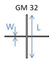
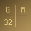
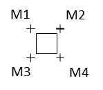
- Global marks: You need at least two wafer marks, a P mark and a Q mark. It is recommended to have many P and Q marks available on the wafer to choose from. The x-coordinate of the P mark should be smaller than the x-coordinate of the Q mark. The global marks should either be crosses or L-shaped, they should be as narrow as possible and 500 - 1000 microns in length. If the wafer contains a number of identical marks, the marks should be marked in order to identify the 'right' alignment mark (the scan width of the SEM is 1 mm x 1 mm). Text around the wafer mark is NOT recommended. Wafer marks formed as crosses with lengths of 1000 microns and 3-5 microns in width are recommended.
- Chip marks: Prepare 1 or 4 chip marks on every chip. The chip marks can be smaller than global marks, as only very fine alignment is performed with chip marks. The chip marks should either be crosses or L-shaped and text around the marks is NOT recommended.

