Specific Process Knowledge/Thin film deposition/Deposition of Niobium Titanium Nitride: Difference between revisions
(→Recipe) |
No edit summary |
||
| Line 1: | Line 1: | ||
Bla bla | |||
* Deposition [[Specific Process Knowledge/Thin film deposition/Deposition of Niobium Titanium Nitride/NbTiN Reactive p-DC Sputtering in Cluster Lesker PC3|Deposition of Niobium Titanium Nitride using reactive p-DC sputtering]] | |||
<i>This page is written by <b>Evgeniy Shkondin @DTU Nanolab</b> if nothing else is stated. <br> | <i>This page is written by <b>Evgeniy Shkondin @DTU Nanolab</b> if nothing else is stated. <br> | ||
All images and photos on this page belongs to <b>DTU Nanolab</b>.<br> | All images and photos on this page belongs to <b>DTU Nanolab</b>.<br> | ||
Revision as of 16:55, 4 October 2023
Bla bla
This page is written by Evgeniy Shkondin @DTU Nanolab if nothing else is stated.
All images and photos on this page belongs to DTU Nanolab.
The fabrication and characterization described below were conducted in 2022 by Evgeniy Shkondin, DTU Nanolab.
This page presents the results of NbTiN deposition using pulsed DC reactive sputtering in Sputter-System Metal-Nitride(PC3), now commonly known as "Cluster Lesker". The deposition target is NbTi 4-inch. Source #1 (RF/p-DC) was used.
The fabrication and characterization described below were conducted in 2022 by Evgeniy Shkondin, DTU Nanolab. The focus of the study was the deposition conditions.
The prepared film was investigated by the X-ray reflectivity, Spectroscopic ellipsometry, X-ray photoelectron spectroscopy and SEM methods. The process recipe is following:
Recipe
The process in a Sputter-System Metal-Nitride(PC3) is based on two recipes:
- Single run recipe:
MD PC3_Src1 - Pulse DC_Downstream with Reactive N2 Gas
- Batch recipe:
MDC PC3_Src1 - Pulse DC_Downstream with reactive N2 and Heating
- Power unit: Power Supply 2 (p-DC)
- Gun: Src1 (4")
- Deposition type: p-DC
- Deposition mode: Downstream
- Power: 500 W.
- Pressure: 3 mTorr
- Ar flow: 20 sccm
- N2 flow: 20 sccm
- Frequency: 100 kHz
- reverse time: 1 µs
- Deposition time: different
- Rotation speed: 10 rpm
- Temperature: 400 C
- Observed DC bias: 450V
- Observed deposition rate: 0.18 nm/s
Process Development
The hysteresis experiment is a valuable method for determining the optimal ratio of working and reactive gases, such as Ar vs. N2 or O2. In this experiment, the flow of the reactive gas is altered while maintaining a constant flow of Ar. Changes in the DC bias are observed and assessed. During the deposition phase, the transition occurs from a 'metallic' to a 'compound' (or 'poisoning') mode and then back. This enables us to determine which gas flow will yield stoichiometric nitride or oxide, and the information about the deposition rate can be utilized for evaluation."
- Hysteresis curve
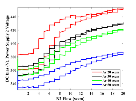
Hysteresis curve for the NbTiN process was generated by gradually increasing the nitrogen flow from 0 sccm to 20 sccm and then back to 0 sccm. The DC bias voltage was observed at each nitrogen flow rate. Throughout the experiment, the power, pressure, and pulse settings remained constant at 500W, 3 mTorr, 100 kHz frequency, and a 1-microsecond reverse time. This experiment was repeated for various values of argon flow.

Spectroscopic Ellipsometry
Spectroscopic ellipsometry was employed to assess the uniformity of thin film thickness and optical properties of NbTiN deposited on a 300 nm dry-oxidized Si wafer. The deposition process involved the following parameters: 500W power, 3 mTorr pressure, 100 kHz frequency, and a 1-microsecond reverse time. The flow rates of Ar and N2 were both maintained at 20 sccm. The deposition duration was 100 seconds, and the temperature was held at 400°C. The analysis was conducted using the Woolam VASE ellipsometer. Drude-Lorentz model was selected in a modelling of NbTiN.
- Ellipsometry results.

Thickness uniformity of NbTiN across 100 mm Si wafer. (Drude-Lorentz model applied).
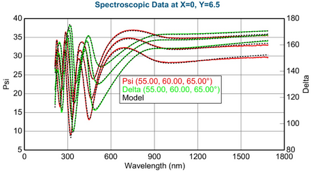
Measured and Fitted Psi-Delta functions.


- Optical functions.
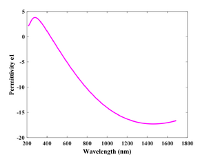
Permittivity e1.
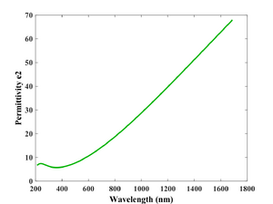
Permittivity e2.
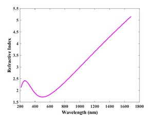
Refractive index.
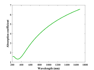
Absorption coefficient.


SEM Measurements
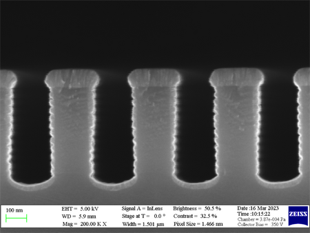
SEM images of deposited NbTiN in Si trench structures. The deposition parameters is given above.
- Scanning Electron Microscopy.
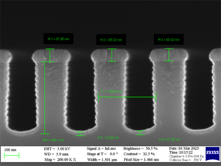
NbTiN
NbTiN
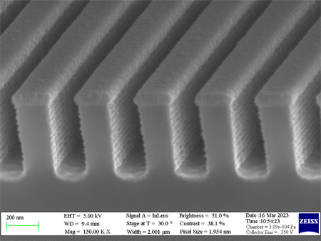
NbTiN tilted view.


XPS Measurements
X-ray photoelectron spectroscopy (XPS) was employed to investigate the chemical composition of deposited NbTiN thin films using the XPS K-alpha instrument. The film was analyzed in a 'depth profile' mode, wherein the film was incrementally etched, and the composition was measured layer by layer. Scans were conducted for survey, O1s, N1s, Ti2p, and Nb3d to gather comprehensive chemical information.
- Scanning Electron Microscopy.
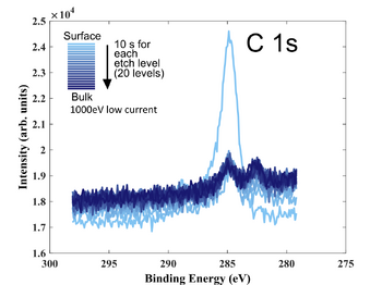
C 1s of NbTiN thin film. High-resolution scan.
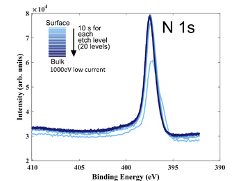
N 1s of NbTiN thin film. High-resolution scan.
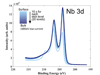
Nb 3d of NbTiN thin film. High-resolution scan.
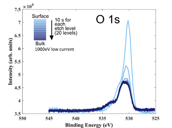
O 1s of NbTiN thin film. High-resolution scan.


- Scanning Electron Microscopy.
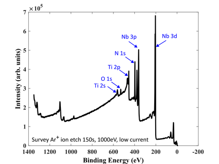
Survey of NbTiN thin film.

Distribution of N,Nb,Ti, and O of NbTiN thin film.


X-ray reflectivity analysis
X-ray reflectivity analysis (XRR) of a sample (NbTiN deposited at 300s, 500W, 439V, 100kHz, 1µs, 3 mTorr, 20 sccm Ar, 20 sccm N2, 400°) have been performed to investigate the thicknesses, roughness, and density profiles.
The scans have been obtained using Rigaku XRD SmartLab equipment. The voltage and current settings for the Cu X-ray tube were standard 40kV and 30mA. The incident optics contained an IPS (incident parallel slit) adaptor with 5 ° Soller slit. Other slits: IS=0.03mm RS1=0.03mm and RS2=0.075mm. Step size: 0.01 and measurement time - 5s for each point. The fitting process was performed using commercial GlobalFit software assuming the model based on Si substrate with native oxide/interlayer followed by the deposited NbTiN film and moisture surfaces. The results are summarized in the tables below.
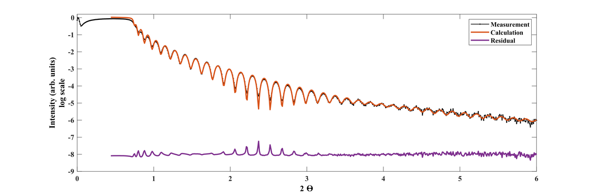
XRR scan of NbTiN deposited at 300s, 500W, 439V, 100kHz, 1µs, 3 mTorr, 20 sccm Ar, 20 sccm N2, 400°.

| XRR results for NbTiN deposited at 300s, 500W, 439V, 100kHz, 1µs, 3 mTorr, 20 sccm Ar, 20 sccm N2, 400° | |||||||||||||||||||||||||||||||||||||||||||||||||||||||||||||||||||||||||||||||||||||||
| |||||||||||||||||||||||||||||||||||||||||||||||||||||||||||||||||||||||||||||||||||||||


