| Date
|
Substrate Information
|
Process Information
|
Results
|
| Wafer info
|
Material/ Exposed area
|
Condi- tioning
|
Recipe
|
Wafer ID
|
Comments
|
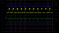
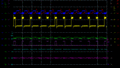
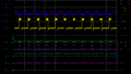
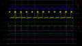
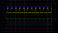
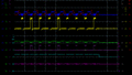
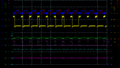
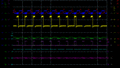
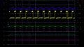
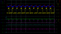
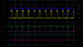
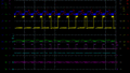
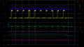
Picoscope
|
Numbers
|
| 27/4-2020
|
Travka05 wafer,
|
Si / 5%
|
S022327 DREM 2kW RF MU runs
|
nanolab/ jmli / DREM / DREM 2kW, 150 cycles or 11:00 minutes
|
S022328
|
Resist etch rate: 62 nm/min Process log entry
|
|
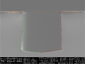
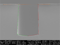
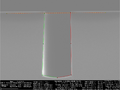
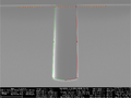
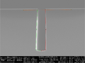
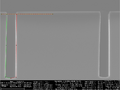
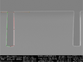
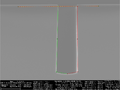
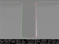
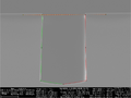
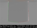
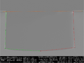
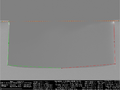
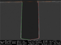
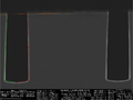
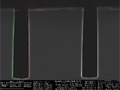
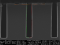
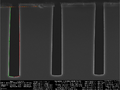
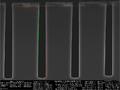
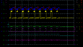
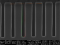
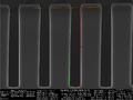
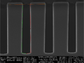
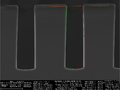
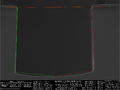
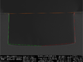
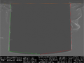
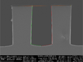
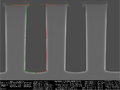
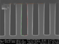
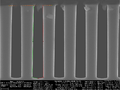
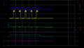
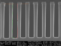
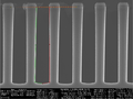
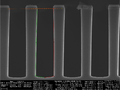
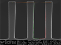
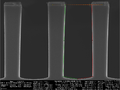
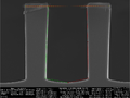
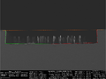
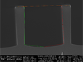
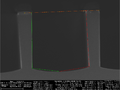
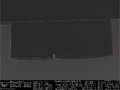
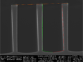
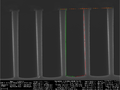
| SEM image:
|
a060
|
a059
|
a058
|
a057
|
a056
|
a055
|
a054
|
a053
|
a052
|
a051
|
a050
|
a049
|
| Trench width (um) |
2.08 |
3.1 |
4.2 |
6.08 |
10.22 |
15.27 |
25.26 |
39.7 |
50.5 |
99.82 |
150.09 |
299.56
|
| Etched depth (um) |
22.96 |
27.05 |
28.46 |
31.57 |
35.48 |
37.96 |
40.7 |
42.39 |
43.24 |
44.09 |
44.54 |
44.56
|
| Etch rate (um/min) |
2.09 |
2.46 |
2.59 |
2.87 |
3.23 |
3.45 |
3.7 |
3.85 |
3.93 |
4.01 |
4.05 |
4.05
|
| Etch rate (nm/cyc) |
153 |
180 |
190 |
210 |
237 |
253 |
271 |
283 |
288 |
294 |
297 |
297
|
| Sidewall bowing (%) |
0.1 |
0.6 |
0.2 |
0.6 |
0.1 |
0.2 |
-0.1 |
0.2 |
-0.4 |
-0.3 |
-0.3 |
-1.1
|
| Sidewall angle (degs) |
90.85 |
90.98 |
90.94 |
91.18 |
91.45 |
91.4 |
91.68 |
92.02 |
91.78 |
92.3 |
92.53 |
92.35
|
| Bottom bowing (%) |
16.93 |
14.87 |
20.32 |
20.1 |
19.02 |
17.6 |
14.71 |
13.78 |
10.7 |
6.84 |
4.53 |
2.34
|
| Aspect ratio |
9.5 |
7.61 |
6.12 |
4.71 |
3.2 |
2.35 |
1.54 |
1.03 |
0.84 |
0.43 |
0.29 |
0.15
|
|
|
|
| .
|
| 27/4-2020
|
Travka10 wafer,
|
Si / 10%
|
S022328 +1min TDESC clean
|
nanolab/ jmli / DREM / DREM 2kW, 150 cycles or 11:00 minutes
|
S022329
|
Resist etch rate: 60 nm/min Process log entry
|
|
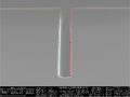
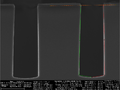
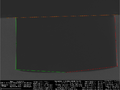
| SEM image:
|
a061
|
a062
|
a063
|
a064
|
a065
|
a066
|
a067
|
a068
|
a069
|
a070
|
a071
|
a072
|
| Trench width (um) |
1.78 |
2.88 |
4.24 |
5.78 |
10.22 |
15.36 |
25.48 |
40.51 |
75.63 |
100.86 |
200.75 |
299.63
|
| Etched depth (um) |
21.26 |
24.82 |
27.54 |
31.1 |
35.34 |
38.21 |
41.17 |
42.98 |
44.58 |
45.15 |
45.16 |
44.68
|
| Etch rate (um/min) |
1.93 |
2.26 |
2.5 |
2.83 |
3.21 |
3.47 |
3.74 |
3.91 |
4.05 |
4.1 |
4.11 |
4.06
|
| Etch rate (nm/cyc) |
142 |
165 |
184 |
207 |
236 |
255 |
274 |
287 |
297 |
301 |
301 |
298
|
| Sidewall bowing (%) |
-0.2 |
0.2 |
-0.1 |
0.2 |
-0.2 |
-0.4 |
-0.2 |
-0.8 |
-0.6 |
-0.7 |
-1.3 |
-1.4
|
| Sidewall angle (degs) |
90.47 |
90.61 |
90.35 |
90.98 |
90.78 |
91.08 |
91.11 |
91.43 |
91.97 |
91.55 |
92.07 |
92.37
|
| Bottom bowing (%) |
26.03 |
15.16 |
18.16 |
17.1 |
17.51 |
17.21 |
15.48 |
13.54 |
8.58 |
6.93 |
3.43 |
2.43
|
| Aspect ratio |
10.89 |
7.92 |
6.26 |
4.94 |
3.31 |
2.38 |
1.57 |
1.04 |
0.58 |
0.44 |
0.22 |
0.15
|
|
|
|
| .
|
| 27/4-2020
|
Travka20 wafer,
|
Si / 20%
|
S022329 +1min TDESC clean
|
nanolab/ jmli / DREM / DREM 2kW, 150 cycles or 11:00 minutes
|
S022330
|
Resist etch rate: 59 nm/min Process log entry
|
|
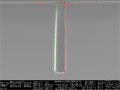
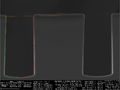
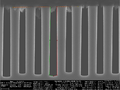
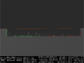
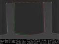
| SEM image:
|
a086
|
a085
|
a084
|
a083
|
a082
|
a081
|
a080
|
a078
|
a077
|
a076
|
a075
|
a074
|
a073
|
| Trench width (um) |
1.91 |
3.04 |
3.68 |
5.89 |
10.08 |
15.02 |
40.03 |
49.99 |
75.51 |
100.03 |
148.99 |
199.75 |
298.84
|
| Etched depth (um) |
21.58 |
24.69 |
26.33 |
29.81 |
33.68 |
36.25 |
40.32 |
40.95 |
41.68 |
41.77 |
41.84 |
42.1 |
41.82
|
| Etch rate (um/min) |
1.96 |
2.24 |
2.39 |
2.71 |
3.06 |
3.3 |
3.67 |
3.72 |
3.79 |
3.8 |
3.8 |
3.83 |
3.8
|
| Etch rate (nm/cyc) |
144 |
165 |
176 |
199 |
225 |
242 |
269 |
273 |
278 |
278 |
279 |
281 |
279
|
| Sidewall bowing (%) |
0.2 |
0.4 |
0.3 |
0.4 |
0.4 |
0.1 |
-0.1 |
-0.5 |
-0.6 |
-0.5 |
-0.6 |
-0.8 |
-0.3
|
| Sidewall angle (degs) |
90.77 |
90.91 |
90.93 |
91.14 |
91.39 |
91.49 |
91.66 |
91.91 |
91.96 |
92.38 |
92.57 |
92.96 |
93.05
|
| Bottom bowing (%) |
23.69 |
15.29 |
19.28 |
16.95 |
17.41 |
17.41 |
12.51 |
11.52 |
8.37 |
6.7 |
4.3 |
3.23 |
2.03
|
| Aspect ratio |
9.8 |
7.2 |
6.42 |
4.6 |
3.1 |
2.28 |
0.98 |
0.8 |
0.54 |
0.41 |
0.28 |
0.21 |
0.14
|
|
|
|
| .
|
| 27/4-2020
|
Travka35 wafer,
|
Si / 35%
|
S022330 +1min TDESC clean
|
nanolab/ jmli / DREM / DREM 2kW, 150 cycles or 11:00 minutes
|
S022331
|
Resist etch rate: 66 nm/min Process log entry
|
|
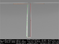
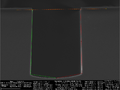
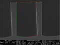
| SEM image:
|
a087
|
a088
|
a089
|
a090
|
a091
|
a092
|
a093
|
a094
|
a095
|
a096
|
a097
|
| Trench width (um) |
1.61 |
2.71 |
3.71 |
7.69 |
9.87 |
15.04 |
25.1 |
40.03 |
75.03 |
199.26 |
299.66
|
| Etched depth (um) |
18.41 |
22.24 |
24.41 |
29.54 |
31.11 |
33.55 |
35.77 |
37.1 |
37.96 |
38.18 |
38.24
|
| Etch rate (um/min) |
1.67 |
2.02 |
2.22 |
2.69 |
2.83 |
3.05 |
3.25 |
3.37 |
3.45 |
3.47 |
3.48
|
| Etch rate (nm/cyc) |
123 |
148 |
163 |
197 |
207 |
224 |
238 |
247 |
253 |
255 |
255
|
| Sidewall bowing (%) |
-0.2 |
0.1 |
0.1 |
0.4 |
0.2 |
0.1 |
-0.3 |
-0.2 |
-0.5 |
-1.1 |
-1.2
|
| Sidewall angle (degs) |
90.33 |
90.75 |
90.89 |
91.13 |
91.07 |
91.31 |
91.34 |
91.69 |
91.84 |
92.49 |
92.44
|
| Bottom bowing (%) |
24.26 |
20.15 |
19.99 |
19.05 |
17.3 |
16.29 |
16.68 |
13.21 |
7.68 |
3.61 |
2.18
|
| Aspect ratio |
10.7 |
7.42 |
5.99 |
3.58 |
2.98 |
2.13 |
1.38 |
0.9 |
0.5 |
0.19 |
0.13
|
|
|
|
| .
|
| 27/4-2020
|
Travka50 wafer,
|
Si / 50%
|
S022331 +1min TDESC clean
|
nanolab/ jmli / DREM / DREM 2kW, 150 cycles or 11:00 minutes
|
S022332
|
Resist etch rate: 58 nm/min Process log entry
|

|
| SEM image:
|
a110
|
a109
|
a108
|
a107
|
a106
|
a105
|
a103
|
a102
|
a101
|
a099
|
a098
|
| Trench width (um) |
1.69 |
2.57 |
3.68 |
7.62 |
14.53 |
39.96 |
49.94 |
100.08 |
199.63 |
298.35 |
299.12
|
| Etched depth (um) |
17.88 |
20.47 |
22.58 |
27.07 |
30.78 |
33.82 |
34.11 |
34.67 |
34.66 |
34.26 |
34.54
|
| Etch rate (um/min) |
1.63 |
1.86 |
2.05 |
2.46 |
2.8 |
3.07 |
3.1 |
3.15 |
3.15 |
3.11 |
3.14
|
| Etch rate (nm/cyc) |
119 |
136 |
151 |
180 |
205 |
225 |
227 |
231 |
231 |
228 |
230
|
| Sidewall bowing (%) |
0.1 |
0.1 |
0.1 |
0.2 |
0.2 |
-0.5 |
-0.3 |
-0.8 |
-0.7 |
-2 |
-1.5
|
| Sidewall angle (degs) |
90.58 |
90.8 |
90.9 |
91.17 |
91.56 |
91.68 |
91.62 |
92.08 |
92.15 |
93.34 |
92.48
|
| Bottom bowing (%) |
24.2 |
20.91 |
19.84 |
16.14 |
17.61 |
12.38 |
10.43 |
5.77 |
3.26 |
1.83 |
1.96
|
| Aspect ratio |
9.58 |
7.18 |
5.61 |
3.32 |
2.01 |
0.83 |
0.67 |
0.34 |
0.17 |
0.11 |
0.11
|
|
|
|
| .
|
| 27/4-2020
|
Travka65 wafer,
|
Si / 65%
|
S022332 +1min TDESC clean
|
nanolab/ jmli / DREM / DREM 2kW, 150 cycles or 11:00 minutes
|
S022333
|
Resist etch rate: 58 nm/min Process log entry
|
|
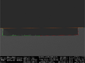
| SEM image:
|
a111
|
a112
|
a113
|
a114
|
a115
|
a116
|
a117
|
a118
|
a119
|
a120
|
a121
|
a122
|
a123
|
a124
|
| Trench width (um) |
2.5 |
3.42 |
5.44 |
7.37 |
9.37 |
14.4 |
24.44 |
39.54 |
74.69 |
100.04 |
150.41 |
199.78 |
299.94 |
301.31
|
| Etched depth (um) |
18.9 |
20.55 |
23.1 |
24.82 |
26.16 |
28.28 |
30.04 |
31.02 |
31.45 |
30.89 |
31.28 |
30.52 |
31.47 |
31.59
|
| Etch rate (um/min) |
1.72 |
1.87 |
2.1 |
2.26 |
2.38 |
2.57 |
2.73 |
2.82 |
2.86 |
2.81 |
2.84 |
2.77 |
2.86 |
2.87
|
| Etch rate (nm/cyc) |
126 |
137 |
154 |
165 |
174 |
189 |
200 |
207 |
210 |
206 |
209 |
203 |
210 |
211
|
| Sidewall bowing (%) |
0 |
0.1 |
0.2 |
0.1 |
0.2 |
0.4 |
0.2 |
-0.3 |
-0.7 |
-1.4 |
-0.7 |
-0.8 |
-0.9 |
-1
|
| Sidewall angle (degs) |
90.75 |
90.75 |
90.96 |
91.03 |
91.19 |
91.48 |
91.42 |
91.86 |
91.99 |
91.88 |
91.81 |
92.79 |
92.54 |
92.34
|
| Bottom bowing (%) |
18.3 |
18.42 |
16.33 |
16.3 |
16.79 |
18.16 |
14.77 |
11.67 |
6.69 |
4.18 |
3.28 |
1.66 |
1.42 |
1.93
|
| Aspect ratio |
6.89 |
5.58 |
3.97 |
3.18 |
2.64 |
1.87 |
1.2 |
0.77 |
0.42 |
0.31 |
0.21 |
0.15 |
0.1 |
0.1
|
|
|
|
| .
|
| 27/4-2020
|
Travka80 wafer,
|
Si / 80%
|
S022333 + 1min TDESC clean
|
nanolab/ jmli / DREM / DREM 2kW nano, 150 cycles or 11:00 minutes
|
S022334
|
Resist etch rate: 79 nm/min Process log entry
|
|
| SEM image:
|
a136
|
a135
|
a134
|
a133
|
a126
|
a125
|
a132
|
a131
|
a130
|
a129
|
a128
|
a127
|
| Trench width (um) |
5.51 |
9.61 |
14.79 |
24.6 |
24.8 |
25.02 |
49.42 |
74.63 |
99.55 |
199.49 |
299.49 |
299.54
|
| Etched depth (um) |
21.45 |
24.21 |
25.99 |
27.45 |
27.15 |
27.35 |
28.03 |
28.38 |
28.48 |
28.23 |
28.52 |
29.16
|
| Etch rate (um/min) |
1.95 |
2.2 |
2.36 |
2.5 |
2.47 |
2.49 |
2.55 |
2.58 |
2.59 |
2.57 |
2.59 |
2.65
|
| Etch rate (nm/cyc) |
143 |
161 |
173 |
183 |
181 |
182 |
187 |
189 |
190 |
188 |
190 |
194
|
| Sidewall bowing (%) |
0.4 |
0.4 |
0.3 |
-0.3 |
-0.1 |
-0.6 |
-0.6 |
-0.7 |
-0.5 |
-1 |
-0.3 |
-1.2
|
| Sidewall angle (degs) |
90.95 |
91.1 |
91.34 |
91.44 |
91.19 |
91.14 |
91.35 |
91.86 |
91.65 |
92.32 |
91.7 |
92.54
|
| Bottom bowing (%) |
13.55 |
16.66 |
16.02 |
14.8 |
13.59 |
14.6 |
8.88 |
5.86 |
4.36 |
2.14 |
1.84 |
1.96
|
| Aspect ratio |
3.66 |
2.41 |
1.69 |
1.09 |
1.07 |
1.07 |
0.56 |
0.38 |
0.28 |
0.14 |
0.09 |
0.1
|
|
|
|
| .
|


