Specific Process Knowledge/Lithography/Aligners/Aligner: Maskless 02 processing: Difference between revisions
| Line 185: | Line 185: | ||
'''Result of using only the alignment tool, pushing it to the extremes:''' | '''Result of using only the alignment tool, pushing it to the extremes:''' | ||
-11.08 to 5.54mRad, corresponding to -0.6 to 0.3°, average -0.1±0.5° | -11.08 to 5.54mRad, corresponding to -0.6 to 0.3°, average -0.1±0.5° | ||
Revision as of 10:52, 12 April 2019
Feedback to this page: click here
THIS PAGE IS UNDER CONSTRUCTION
Exposure technology
Aligner: Maskless 02 is not a direct writer. In the maskless aligner, the exposure light is passed through a spatial light modulator, much like in a video projector, and projected onto the substrate, thus exposing an area of the design at a time. The substrate is exposed by scanning the exposure field across the substrate in a succession of stripes.
The light source is a laser diode (array) with a wavelength of 375nm (2.8W) or 405nm (8W). The spacial light modulator is a digital micro-mirror device. The individual mirrors of the DMD are switched in order to represent the design, and the laser is flashed in order to yield the desired exposure dose. This image is projected onto the substrate through a lens(system). The projected image yields a pixel size of 160nm X 160nm at wafer scale. The image is scanned across the substrate, in order to expose the entire design, each stripe overlapping (2 or 4 times) in order to minimize uniformity effects and stitching errors.
The writing head of the Aligner: Maskless 02 moves only in the z-direction. Using an optical (or pneumatic) focusing system, the maskless aligner is able to do real-time autofocus. The defocus process parameter is used to compensate offsets in the focusing mechanism, and to optimize printing quality in different resists and varying thicknesses. The stage of the Aligner: Maskless 02 moves only in x and y. It has no theta-axis. All rotation during alignment is thus accomplished by transformation of the input design.
Process Parameters
The lithographic result of exposure on Aligner: Maskless 02 depends on a lot of factors, including the dose and defocus parameters, and the exposure mode used. The optimal dose and defocus depend on the type and thickness of the resist, and the optical properties of the substrate (e.g. reflective/absorbing/transparent). All of these factors influence the obtainable resolution, as well as the writing speed.
The correct way to determine the best dose-defocus settings is to generate a so-called Bossung plot (known from projection lithography), which plots the printed linewidth as a function of dose and defocus. From this, the most stable region of parameter space is chosen, i.e. the region where the linewidth changes the least when dose and defocus changes. Any deviation from the design linewidth can be corrected using the CD bias parameter. This typically involves SEM imaging of resist cross-sections, and quickly becomes time consuming. However, in most cases, inspection of a dose-defocus matrix (easily generated using the series exposure function) in an optical microscope will get you most of the way.
Exposure dose
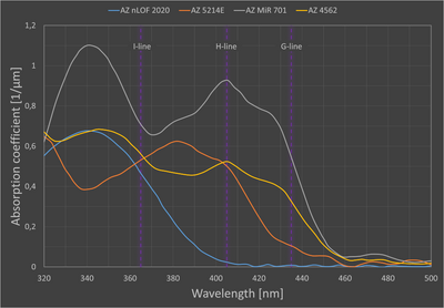
Exposure dose relative to exposure at 365nm (Aligner: Maskless 01):
| 375nm | 405nm | |
|---|---|---|
| AZ 5214E | 0.95 | 1.3 |
| AZ 4562 | ? | ? |
| AZ MiR 701 | 1 | 1.2 |
| AZ nLOF 2020 | 3 | NA |
| SU-8 | 10-15 | NA |
Defocus
Optical
Pneumatic
Exposure mode
Aligner: Maskless 02 offers two exposure modes.
High quality (4) mode is used for optimal resolution and minimum stripe stitching effects. In the high quality mode, an area of the pattern is exposed by 4 stripes, each 160µm wide and exposing a quarter of the dose. At the same time, sub-pixel interpolation is applied, yielding an address grid size of 40nm.
Fast mode is used for maximum exposure speed. In the fast mode, each area of the pattern is exposed by 2 stripes only. This effectively cuts the exposure time in half, but also doubles the size of the address grid in the X-direction. Due to less averaging of non-uniformities, stitching effects will be more prominent in this mode.
Resolution
- 5206E 0.5µm 375nm, dev 2xSP30s
Fast: 60mJ/cm2; defoc -6 (1µm, not optimized)
Quality: 60mJ/cm2; defoc -6 (~750nm, not optimized)
- 5214E 1.5µm 405nm, dev SP60s
Fast: 90mJ/cm2; defoc -2 (1-2µm)
- 5214E 1.5µm 375nm, dev SP60s
Fast: 65mJ/cm2; defoc 2 (~1µm)
Quality: 65mJ/cm2; defoc 2 (~750nm)
- MiR 701 1.5µm 405nm, PEB 60s@110°C dev SP60s
Fast: 200mJ/cm2; defoc -5 (~1µm, not optimized)
- MiR 701 1.5µm 375nm, PEB 60s@110°C dev SP60s
Fast: 170mJ/cm2; defoc -5 (1µm)
Quality: 180mJ/cm2; defoc -6 (750nm)
- nLOF 2020 2µm 375nm, PEB 60s@110°C dev SP60s
Fast: 400mJ/cm2; defoc 5 (~1µm, not optimized)
Quality: 400mJ/cm2; defoc 0 (1µm)
Writing speed
According to specs, the writing speed of Aligner: Maskless 02 is 285mm2/min in fast mode. Using the high quality exposure mode cuts this speed in half, to approximately 140mm2/min. The writing speed for a 100x100mm2 area measured during installation of the machine (acceptance test) was ~340mm2/min for both exposure wavelengths.
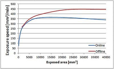
- Speed vs. area (375nm)
- Online
- Offline
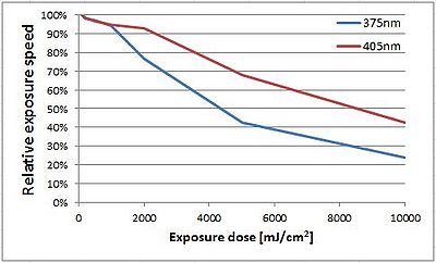
- Speed vs. dose (375nm + 405nm)
- Speed vs. design
Features
Substrate centring and flat alignment
During substrate detection, the sample is scanned along the X- and Y-axes, as well as diagonally. From these measurements, the size (diameter) of the substrate is calculated, as well as the stage position matching the center of the substrate. This stage position will be the default origin for the subsequent exposure.
At the end of substrate detection, the sample is scanned twice along the bottom edge (flat), in order to determine the substrate rotation. This angle will be presented in the exposure panel along with the option to expose the design rotated in order to compensate for this angle, i.e. aligned to the flat/edge of the substrate.
Result of using "Expose with substrate angle" on three samples with optical autofocus:
- Rotation: 0.5±0.2°
- Centering:
- X 100±250µm
- Y 200±250µm
The error on the flat alignment is surprising when compared to the 0±0.1° measured on Aligner: Maskless 01. The centring, on the other hand, is seen to be within a few hundred µm, without correcting for the flats.
Result of loading the same substrate 2x9 times without removing it from the stage:
| Average | Range | |
|---|---|---|
| Optical
autofocus |
3.7 mRad | ±13.9 mRad
±0.8° |
| Pneumatic
autofocus |
-3.1 mRad | ±1.4 mRad
±0.08° |
Result of using only the alignment tool, pushing it to the extremes:
-11.08 to 5.54mRad, corresponding to -0.6 to 0.3°, average -0.1±0.5°
Labeling
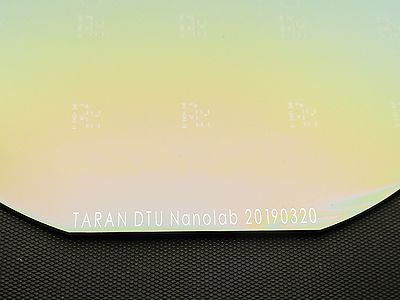
The conversion manager software allows for inclusion of labels during the design conversion process. The labels are configured in a .lbl tab-delimited ASCII file with a special header in the first row, which must be located in HIMT\Designs\Labels folder. When used, the labels defined in the label file will be merged with the pattern in the source file, and the result can be inspected in the viewer. The X and Y positions of the labels should be given in design coordinates, and will be subject to any offsets/shifts applied to the design. Note, that if the label file is changed, the job file will not update automatically.
Example of a label file:
X | Y | UNIT | HEIGHT | UNIT | TITLE
-16000 | -46000 | um | 2000 | um | TARAN DTU Nanolab 20190320
This produces a 2mm high, approximately 32mm long wafer ID at the flat of a 4" wafer. Some special characters are not allowed (e.g. ';').
Large defocus range??
High Aspect Ratio (DOF) mode
Aligner: Maskless 02 is configured with the so-called "Write Mode I", which uses a higher demagnification, higher NA lens system to achieve higher resolution. This reduces the depth of focus (technically depth of field), making it more difficult to achieve good lithographic results in thicker resist coatings. The theoretical DOF of Aligner: Maskless 02 is 0.3µm, compared to 1µm for Aligner: Maskless 01. In order to enable processing of thick resists, the Aligner: Maskless 02 has been configured with the High Aspect Ratio Mode, which uses a variable aperture in the optical path to decrease the (illumination) NA of the system, thus increasing the DOF at the expense of intensity and resolution limit.
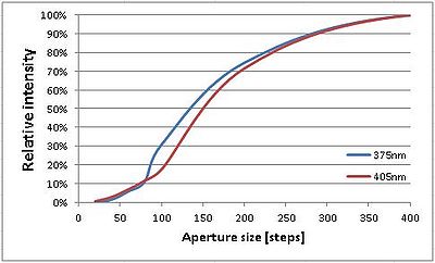
In High AR mode, the aperture size is controlled via a parameter in the resist template. The high AR parameter can be Standard (aperture fully open; 800 motor steps), Large (100 steps), or X-Large (60 steps). Assuming a linear relation between motor steps and aperture diameter, Large corresponds to a relative aperture area of 1.6%, while X-Large corresponds to 0.6% aperture area. Intensity measurements show a relative intensity of approximately 25%, and 6%, respectively. The effective dose can be corrected by increasing the nominal dose in the exposure, either by a fixed machine parameter, or by the user setting a higher dose themselves. At the moment, the user will be required to increase the nominal dose.
Decreasing the aperture size significantly reduces the amount of light that reaches the sample, and thus the effective dose, as can be seen in the graph to the right, and the table below. The resolution limit, however, seem to be much less affected. Tests using 1.5µm MiR resist suggest that using the X-Large setting (60 steps) reduces the achievable resolution from 1µm at Standard setting to 3µm for exposure at 375nm, but only to 1.75µm for exposure at 405nm.
Dose factor for different wavelengths and aperture settings:
| 375nm | 405nm | |||
|---|---|---|---|---|
| Large (100) | X-Large (60) | Large (100) | X-Large (60) | |
| Intensity measurements | 3.3 | 17.4 | 5.7 | 14.6 |
| 150µm SU-8 acceptance test | ~3 | ~10 | NA | NA |
| 1.5µm AZ MiR 701 dose test | 7.5 | 20.8 | 6.7 | 18.0 |
| 10µm AZ 4562 dose test | ? | ? | ? | ? |
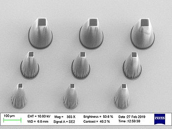
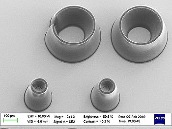
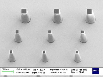
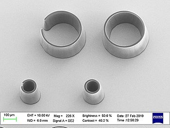
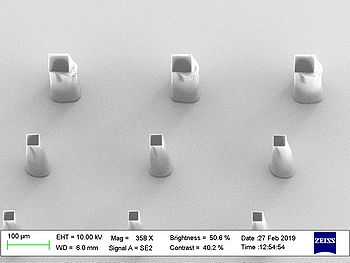
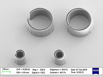
Results from acceptance test on 150µm thick SU-8:
| Pillars | Rings | |
|---|---|---|
| Standard (800)
6000 mJ/cm2 |
|
|
| Large (100)
16500 mJ/cm2 |
|
|
| X-Large (60)
55000 mJ/cm2 |
|
|
Alignment
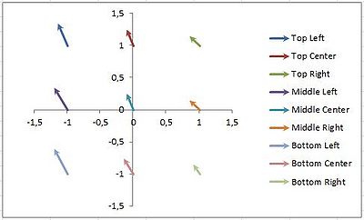
Stage stitching test:
| Shift (median) [µm] | Misplacement [µm] | Run-out (gain) [ppm] | Rotation [ppm] | ||
|---|---|---|---|---|---|
| 9 points, 60x60mm2 | X | -0.15±0.05 | -0.16±0.05 | 0.8±1.7 | -3.6±1.2 |
| Y | 0.25±0.125 | 0.26±0.11 | -0.3±1.7 | -0.3±1.2 | |
| All 25 points | X | -0.150±0.075 | |||
| Y | 0.250±0.125 | ||||
Top Side Alignment
Camera field of view (W x H):
High Res 64µm x 48µm
Low Res 213µm x 160µm
Overview 13mm x 10mm
- 4 marks (before final installation)
- Scaling (375nm, high res camera)
| MLA-MLA | Scaling [ppm] | Shearing [mRad] | Shift (median) [µm] | Misplacement [µm] | Run-out (gain) [ppm] | Rotation [ppm] | |
|---|---|---|---|---|---|---|---|
| 2 alignment marks
375nm, high res camera |
X | NA | NA | 0.0±0.05 | 0.0±0.05 | 0.0±1.18 | 0.0±1.67 |
| Y | NA | 0.0±0.05 | 0.0±0.05 | 0.0±1.18 | 0.0±1.67 | ||
| 4 alignment marks
375nm, high res camera |
X | 0±0 | 0.000±0.000 | 0.0±0.05 | 0.0±0.05 | 0.0±1.18 | 0.0±1.67 |
| Y | 0±0 | 0.0±0.05 | 0.0±0.05 | 0.0±1.18 | 0.0±1.67 | ||
| 4 alignment marks
405nm, high res camera |
X | 0±0 | 0.000±0.000 | 0.0±0.05 | 0.0±0.05 | 0.0±1.18 | 0.0±1.67 |
| Y | 0±0 | 0.0±0.05 | 0.0±0.05 | 0.0±1.18 | 0.0±1.67 | ||
Scaled first print:
| MLA-MLA | Scaling [ppm] | Shearing [mRad] | Shift (median) [µm] | Misplacement [µm] | Run-out (gain) [ppm] | Rotation [ppm] | |
|---|---|---|---|---|---|---|---|
| 4 alignment marks
375nm, high res camera |
X | 100 | 0.000 | -0.05±0.1 | -0.01±0.05 | 1.7±3.3 | 0.6±2.4 |
| Y | 101 | 0.2±0.05 | 0.18±0.05 | 0±3.3 | 0±2.4 | ||
| 4 alignment marks
375nm, high res camera |
X | not used | not used | -2.75±3.0 | -2.98±0.05 | -101±1.7 | -0.6±1.2 |
| Y | not used | 3.0±2.9 | 3.12±0.05 | -96.1±1.7 | 0.0±1.2 | ||
Back Side Alignment
BSA windows: along the X and Y axes, 10mm x 46mm, starting 14.5mm from the center.
Camera field of view (W x H): 640µm x 480µm
- Tested, 2-3µm error in X observed
- Corrected
| Offset [µm] | ||
|---|---|---|
| Align-flip180-align, 1 point | X | 0.25±0.25 |
| Y | 0.25±0.25 | |
| KOH-window | X | 0.0±0.5 |
| Y | 0.0±0.5 | |
Advanced Field alignment (TSA)
- 4 marks, 25 fields (375nm, high res camera)
- Scaled first print, 10 fields (375nm, high res camera)
- 4 marks, 25 fields (405nm, high res camera)
| Shift (median) [nm] | Misplacement [nm] | ||
|---|---|---|---|
| 25 fields
375nm, high res camera |
X | 50±75 | 70±75 |
| Y | 150±50 | 128±50 | |
| Scaled first print, 10 fields
375nm, high res camera |
X | -25±50 | -5±50 |
| Y | 100±50 | 120±50 | |
| 25 fields
405nm, high res camera |
X | 100±75 | 108±75 |
| Y | 0±50 | 16±50 | |
