LabAdviser/Technology Research/Nanoscale characterization of ultra-thin metal films for nanofabrication applications: Difference between revisions
| Line 20: | Line 20: | ||
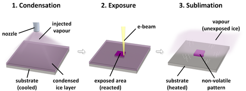
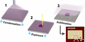
[[image:ProcessOIR.png|500px|thumb|Lithography process for Organic Ice Resists]] | [[image:ProcessOIR.png|500px|thumb|Lithography process for Organic Ice Resists]] | ||
The deposition of metal thin- | The deposition of metal thin-film structures on dielectric or semiconductor substrates is central for the fabrication of structures and devices having nanoscale characteristic dimension. With the constant miniaturization of the devices and the fabrication of increasingly complex multi-material structures, the interaction between different ultra-thin layers has gained considerable importance in the field of thin-film science and technology in recent years. Therefore the characterization of such interactions in a wide range of temperatures and the description of their impact on the chemical composition, morphology and distribution of crystallographic orientations of multilayer thin-films is of utmost importance. | ||
This Phd project focuses on the description of the interaction at the nanoscale level between noble metal �films, widely used in different areas of micro- and nanofabrication, and extremely thin �films of reactive transition metals, used to enhance adhesion onto the substrate - and thus referred as "adhesion layers". In particular, the work focused on the study of pure Au �films and Cr/Au and Ti/Au systems, which were analyzed at different temperatures using a spectrum of complementary characterization techniques. | This Phd project focuses on the description of the interaction at the nanoscale level between noble metal �films, widely used in different areas of micro- and nanofabrication, and extremely thin �films of reactive transition metals, used to enhance adhesion onto the substrate - and thus referred as "adhesion layers". In particular, the work focused on the study of pure Au �films and Cr/Au and Ti/Au systems, which were analyzed at different temperatures using a spectrum of complementary characterization techniques. | ||
Revision as of 15:51, 4 July 2018
Feedback to this page: click here
Nanoscale characterization of ultra-thin metal films for nanofabrication applications
- Project type: Ph.D. project
- Project responsible: Matteo Todeschini
- Supervisors: Jakob Birkedal Wagner, Flemming Jensen, Anpan Han
- Partners involved: DTU Danchip/Cen
Nanoscale characterization of ultra-thin metal films for nanofabrication applications
- Project type: Ph.D. project
- Project responsible: Matteo Todeschini (DTU Orbit)
- Supervisors: Prof. Jakob Birkedal Wagner, Assoc. Prof. Flemming Jensen, Assist. Prof. Anpan Han
- Partners involved: DTU Danchip/Cen
- Full thesis: Link
- Overview: Electron-Beam Lithography on Organic Ice Resists
- Overview: SEM-LEO Customizations for Organic Ice Resists
Project Description

The deposition of metal thin-film structures on dielectric or semiconductor substrates is central for the fabrication of structures and devices having nanoscale characteristic dimension. With the constant miniaturization of the devices and the fabrication of increasingly complex multi-material structures, the interaction between different ultra-thin layers has gained considerable importance in the field of thin-film science and technology in recent years. Therefore the characterization of such interactions in a wide range of temperatures and the description of their impact on the chemical composition, morphology and distribution of crystallographic orientations of multilayer thin-films is of utmost importance.
This Phd project focuses on the description of the interaction at the nanoscale level between noble metal �films, widely used in different areas of micro- and nanofabrication, and extremely thin �films of reactive transition metals, used to enhance adhesion onto the substrate - and thus referred as "adhesion layers". In particular, the work focused on the study of pure Au �films and Cr/Au and Ti/Au systems, which were analyzed at different temperatures using a spectrum of complementary characterization techniques.
The project involved the introduction of the recently developed transmission Kikuchi diffraction (TKD) technique for the characterization of the crystal structure, grain size, and crystallographic texture of polycrystalline thin �films. The remarkable potential of TKD for the in-situ analysis of thin �films at elevated temperatures was revealed through the in-situ investigation of solid-state dewetting of Au, enabling to observe the start of the dewetting at a temperature as low as 150°C and demonstrating the crucial role of temperature in the modi�cation of the nanostructure of metal thin �films during nanofabrication. The data acquired during solid state dewetting were used to qualitatively study the formation and expansion of the holes in the �film. A new criterion for the detection of the temperature of formation of the holes in the �film was introduced and an in-situ monitoring of the formation and expansion of the holes in the Au �film was also performed. This allowed to observe the formation of the holes exclusively in the positions of high surface energy grains and the reduction of the interface energy of the system by the elimination of grain boundaries and by grain coalescence.
Dissemination
Publications in Peer Reviewed Journals
- Organic Ice Resists

- Link to Article
- W. Tiddi, A. Elsukova, H. T. Le, P. Liu, M. Beleggia, and A. Han
Nano Letters, vol. 17, pp. 7886-7891, 2017.
- Organic ice resists for 3D electron-beam processing - Instrumentation and operation

- Link to Article
- W. Tiddi, A. Elsukova, M. Beleggia, and A. Han
Microelectronic Engineering, vol. 192, pp. 38-43, 2018.
- Inductively coupled plasma nanoetching of atomic layer deposition alumina

- Link to Article
- A. Han, B. Chang, M. Todeschini, H. T. Le, W. Tiddi and M. Keil
Microelectronic Engineering, vol. 193, pp. 28-33, 2018.
Published Patents
- A METHOD FOR CREATING STRUCTURES OR DEVICES USING AN ORGANIC ICE RESIST.
- Link to Patent Database
- A. Han (Inventor), W. Tiddi (Inventor), M. Beleggia (Inventor)
IPC No.: B29C 67/ 00 A I. Patent No.: WO2017191079. Nov 09, 2017.
Conferences and Workshops Contributions
- Organic ice resists - condensed small molecules as spin-free volatile E-beam resists
- W. Tiddi, A. Elsukova, H. T. Le, M. Beleggia, and A. Han
Oral presentation at 43rd International conference on Micro and Nano Engineering, Braga, Portugal, 2017.
- Ice lithography - ice-based nanopatterning
- W. Tiddi
Workshop lecture at Nordic Nanolab User Meeting 2017, Trondheim, Norway, 2017.
- Advances in Ice Lithography in Denmark and China
- W. Tiddi, D. Zhao, M. Qiu, M. Beleggia, and A. Han
Abstract and Poster at 42nd International conference on Micro and Nano Engineering, Vienna, Austria, 2016.
- Ice lithography - water-based nanopatterning.
- W. Tiddi, M. Beleggia, and A. Han
Abstract and Poster at Sustain-ATV Conference 2016, Kgs. Lyngby, Denmark, 2016.
- Proximity Effects in a Chemically Amplified Electron Beam Resist Patterned at 100 keV.
- W. Tiddi, T. Greibe, M. Beleggia, and A. Han
Abstract and Poster at 41st International conference on Micro and Nano Engineering, The Hague, Netherlands, 2015.
