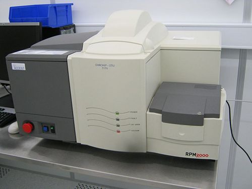
Specific Process Knowledge/Characterization/PL mapper: Difference between revisions
Appearance
Created page with "'''Feedback to this page''': '''[mailto:danchipsupport@danchip.dtu.dk?Subject=Feed%20back%20from%20page%20http://labadviser.danchip.dtu.dk/index.php?title=Specific_Process_Kno..." |
|||
| Line 4: | Line 4: | ||
Photoluminiscense mapping is a non-contact, non-destructive technique for mapping out uniformity of alloy composition, material quality and defects in substrates and of III-V epiwafers. The Rapid Photoluminiscense Mapper (RPM) is equipped with 3 lasers for PL measurements and a white-light source to map out thickness and reflectance of eg layers, microcavities and VCSELs. | Photoluminiscense mapping is a non-contact, non-destructive technique for mapping out uniformity of alloy composition, material quality and defects in substrates and of III-V epiwafers. The Rapid Photoluminiscense Mapper (RPM) is equipped with 3 lasers for PL measurements and a white-light source to map out thickness and reflectance of eg layers, microcavities and VCSELs. | ||
It can also be used to map out voids after silicon wafer-bonding. This is done using the reflectance mapping and is using the fact that silicon is transparent for wavelengths above ~1000nm. A void will therefor change the reflectance in that wavelength range. | |||
Revision as of 15:54, 24 March 2017
Feedback to this page: click here
PhotoLuminescense Mapper RPM2000
Photoluminiscense mapping is a non-contact, non-destructive technique for mapping out uniformity of alloy composition, material quality and defects in substrates and of III-V epiwafers. The Rapid Photoluminiscense Mapper (RPM) is equipped with 3 lasers for PL measurements and a white-light source to map out thickness and reflectance of eg layers, microcavities and VCSELs.
It can also be used to map out voids after silicon wafer-bonding. This is done using the reflectance mapping and is using the fact that silicon is transparent for wavelengths above ~1000nm. A void will therefor change the reflectance in that wavelength range.
The user manual and contact information can be found in LabManager:

| Performance | Excitation |
|
|---|---|---|
| Detection |
| |
| Gratings |
| |
| Chuck sizes |
| |
| Resolution |
| |
| Wavelength accuracy |
| |
| Materials | Allowed substrate materials |
|
| Forbidden materials |
| |
| Software | RPM viewer |
|
