LabAdviser/Technology Research/Nanofabrication of Inductive Components for Integrated Power Supply On Chip: Difference between revisions
No edit summary |
|||
| Line 16: | Line 16: | ||
[[image:Untitled4.png| | [[image:Untitled4.png|750px]] | ||
Power supply in package using TSV-based inductive interposers | Power supply in package using TSV-based inductive interposers | ||
| Line 30: | Line 30: | ||
'''Full thesis''': [[:File:1. A4size_HoaThanhLe_Thesis_14.12.2017.pdf]] | '''Full thesis''': [[:File:1. A4size_HoaThanhLe_Thesis_14.12.2017.pdf]] | ||
=Dissemination= | =Dissemination= | ||
Revision as of 15:39, 5 March 2019
Feedback to this page: click here
Nanofabrication of Inductive Components for Integrated Power Supply On Chip
- Project type: Ph.d project
- Project responsible: Hoà Lê Thanh
- Supervisors: Flemming Jensen (Main), Anpan Han (Co), Ziwei Ouyang (Co), Arnold Knott (CO)
- Partners involved: DTU Danchip, DTU Elektro
Project description
Power supplies are essential sub-systems to power electronic devices. They can be found in almost all electronic devices, from traditional electrical devices such as cars, televisions, CD players, and cellular phones to modern intelligent electronic devices and systems such as wearable devices, light emitting diode (LED) applications, and internet of things (IoTs)2. As more functions are packed in a limited space in such electronic systems, power supplies are required to be more compact and more efficient with a lower manufacture cost. Hence, miniaturization has become the main trend for developing future generation of power supplies.
One way of miniaturization is monolithic integration of power supplies or so-called power supply on chip (PwrSoC). The PwrSoC vision is to integrate all active and passive power electronics components on one chip. Higher integration lowers the cost and increases both efficiency and power density. On the evolution route towards PwrSoC, the intermediate short-term solution is power supply in package (PSiP) in which the discrete inductors and capacitors are co-packaged together with the power management integrated circuits. SMPS, which incorporate a switching regulator to convert electrical power efficiently, are widely investigated for PSiP and PwrSoC due to its high efficiency and high power density. It is evident that the development of such integrated SMPS will play an important role in future civilization and also in the fight against climate change. A challenge for developing integrated SMPS is to miniaturize bulky energy-storing elements e.g. inductors. Inductors are by far the most bulky and lossy components in the SMPS circuits, therefore, miniaturizing power inductors is needed. One route is to increase the switching frequency of SMPS that enables the use of smaller inductors with lower inductance value, thus reducing the overall size of SMPS. The evolution of integrated power supplies is highly correlated to the increase in the switching frequency, for example 8 - 20 MHz for co-packaged or stacked PSiP and to 30 - 300 MHz of VHF range for PwrSoC. Microelectromechanical systems (MEMS) technology is a promising solution that has a great potential for heterogeneous integration of microinductors.
Power supply in package using TSV-based inductive interposers
Project type: Ph.D. project
Project responsible: Hoa Thanh Le ([1])
Supervisors: Assoc. Prof. Flemming Jensen, Assoc. Prof. Anpan Han, Assoc. Prof. Ziwei Ouyang, Assoc. Prof. Arnold Knott,
Partners involved: DTU Danchip/Cen, DTU ELektro
Full thesis: File:1. A4size_HoaThanhLe_Thesis_14.12.2017.pdf
Dissemination
[1] Hoa Thanh Le, Io Mizushima, Peter Torben Tang, Ziwei Ouyang, Flemming Jensen, and Anpan Han. “Fabrication of 3D Air-core MEMS Inductors for High Frequency Power Electronic Applications”. Microsystems & Nanoengineering, vol. 4, no. 17082, 2018. ([2])
[2] Hoa Thanh Le, Yasser Nour, Anpan Han, Flemming Jensen, Ziwei Ouyang, and Arnold Knott, “Microfabricated Air-core Toroidal Inductor In Very High Frequency Power Converters” IEEE Journal of Emerging and Selected Topics in Power Electronics, Vol. 6, no. 2, pp. 604 – 613, 2018. ([3])
[3] Hoa Thanh Le, Yasser Nour, Cian O Mathuna, Flemming Jensen, Santosh Kulkarni, Anpan Han, Ziwei Ouyang, “High-Q 3D Microfabricated Magnetic-core Toroidal Inductors for Power Supplies in Package”, IEEE Transaction on Power Electronics, 10.1109/TPEL.2018.2847439, 2018. ([4])
[4] Hoa Thanh Le, Yasser Nour, Flemming Jensen, Anpan Han, Arnold Knott, Santosh Kulkarni, Ziwei Ouyang, “Microfabricated 3D Toroidal Inductors Using A Novel Magnetic System”, unpublished (awaiting for the patent application to be filed).
[5] Hoa Thanh Le, Yasser Nour, Flemming Jensen, Anpan Han, Arnold Knott, Ziwei Ouyang, “Integrated Power Supply in Package (PSiP) using Inductive Interposer”, unpublished.
[6] William Tiddi, Anna Elsukova, Hoa Thanh Le, Pei Liu, Marco Beleggia, Anpan Han, “Organic ice resists”, Nanoletters, vol. 17, no. 12, pp. 7886–7891, 2017 ([5])
[7] Anpan Han, Bingdong Chang, Matteo Todeschini, Hoa Thanh Le, William Tiddi, Matthias Keil, “Inductively coupled plasma nanoetching of atomic layer deposition alumina”, Microelectronic Engineering, Vol. 193, no. 5, pp. 28-33, 2018. ([6])
Fabrication Process Flow
Process flow:
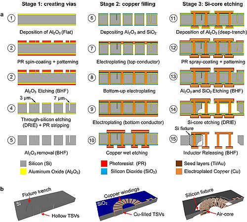
Stage 1 focuses on DRIE TSV etching, and it starts with Step 1 of depositing 50-nm-thick aluminium oxide (Al2O3) on both wafer sides by atomic layer deposition (ALD). In Step 2, on the wafer front side, an Al2O3 hard mask is patterned by buffered hydrofluoric acid (BHF) etch using a photoresist mask (AZ MiR 701). Next, TSVs are created by DRIE. The aspect ratio is from 9 to 12. The core shape is also defined in this step by the fixture trenches, which is between 3 and 7 µm. Finally, the remained resist and Al2O3 are removed with oxygen plasma and BHF. Stage 1 is finalized by an RCA cleaning step, which is an important preparation for stage 2.
Stage 2 focuses on creating Cu TSVs and windings. First, in Step 6, Al2O3 is deposited, since it is crucial to cover and protect deep fixture trenches (aspect ratio > 30) during Si core removal (stage 3). Because of the high etching selectivity for Si over Al2O3 in an SF6 plasma (100 000:1) only 50 nm of Al2O3 thin-film is sufficient to protect the Si support and fixtures while removing the Si core. Step 6 also includes the deposition of 1.5 µm SiO2 by plasma enhanced chemical deposition (PECVD) which partly seals the 3-µm-wide fixture trenches to avoid defects on the top windings. Subsequently, three electroplating steps to form Cu windings are done. A 30-µm-thick top layer is fiµrst plated to seal the TSVs (step 7) followed by a bottom-up plating step to all the TSVs (step 8), and finally a 30-µm-thick bottom layer (step 9) is plated. For the electroplating seed layer, we use an electron beam evaporated 10 nm Cr and 100 nm Au thin-film stack. The inductor windings are patterned by Cu wet-etching using a resist mask, thus obtaining the Si-core inductor (step 10).
In stage 3, etching mask for Si-core removal is patterned by photolithography on spraycoated resist and buffered hydrofluoric acid (BHF) wet etching. This stage is divided into two parts: patterning etching mask and etching the Si core. In the first part, ALD Al2O3 and 4-µm AZ4562 are used as etching mask. In step 11, a 50 nm Al2O3 layer is firstly deposited. Protecting this Al2O3 layer is crucial to have well-defined Si fixtures and Si support die. In step 12, spray coating is utilized to coat a conformal resist layer on Cu windings (30 -50-µm-thick ), and more importantly to seal the 3-µm and 7-µm fixture trenches. In step 13, Al2O3 and SiO2 are etched by BHF wet etching to expose the silicon (step 13) for Si-core removal. In the second part, the Si core is selectively removed by inductively coupled plasma (ICP) etching (step 14). During the ICP etch, Cu is protected by the 50-nm-thick Al2O3 layer from the plasma environment as an additional precaution. Al2O3 layers deposited on the fixture trenches and at the wafer backside acts as an ICP etch stop, allowing complete removal of the Si core. The windings are anchored by several Si fixtures and suspended on the Al2O3/SiO2 membrane. The final air-core inductor is obtained by removing the oxides in BHF (step 15).
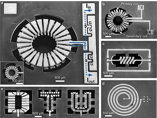
Fabricated Microinductors: SEM micrographs of MEMS air-core inductors, (a) toroidal inductors with 16 mm2 (1.5 mm outer radius, 0.75 mm inner radius, 25 turns) and 4 mm2 footprint (inset) Presented by the lines and arrows, the current fows from the top wire bonding pad, through the TSV interconnects, then passing through the windings and exits at the lower pad. The measurement pads are designed in ground-signal-ground (GSG)
configuration at both terminals for wafer-level probing. Four 800 µm by 800 µm pads at the corners are for flip-chip bonding. (b) 1:1 toroidal transformer. The primary coil has larger conductors than that of the secondary coil. (c) solenoid inductor, (d) spiral inductor, (e) "DTU" inductor.
SEM micrographs of MEMS air-core inductors, (a) toroidal inductors with 16 mm2 (1.5 mm outer radius, 0.75 mm inner radius, 25 turns) and 4 mm2 footprint (inset) Presented by the lines and arrows, the current ows from the top wire bonding pad, through the TSV interconnects, then passing through the windings and exits at the lower pad. The measurement pads are designed in ground-signal-ground (GSG) configuration at both terminals for wafer-level probing. Four 800 µm by 800 µm pads at the corners are for flip-chip bonding. (b) 1:1 toroidal transformer. The primary coil has larger conductors than that of the secondary coil. (c) solenoid inductor, (d) spiral inductor, (e) \DTU" inductor.


