Specific Process Knowledge/Etch/DRIE-Pegasus/TrenchCharacterisation: Difference between revisions
| Line 9: | Line 9: | ||
=== Input parameters === | === Input parameters === | ||
Many users make measurements using the annotations in the SEM. However, instead of adding a ton of measurements to each SEM image while at the SEM and hence spend an unreasonable amount of time there, one can postpone making the measurements till afterwards. The only requirement is that the pixel size of every SEM image is known - one can add it to the datazone: See any SEM manual for instructions. | Many users make measurements using the annotations in the SEM. However, instead of adding a ton of measurements to each SEM image while at the SEM and hence spend an unreasonable amount of time there, one can postpone making the measurements till afterwards. The only requirement is that the pixel size of every SEM image is known - one can add it to the datazone: See any SEM manual for instructions - for instance [http://labmanager.dtu.dk/d4Show.php?id=2180&mach=275#dafs29430 '''HERE'''] | ||
: Opening the images with Irfanview (or any other image viewer with the same possibilities) and drawing squares (the pixel dimensions are shown in the top) as measurements. These squares are one pixel wide compared to the 2 (or even 3) which are default for the annotations in smartSEM. | : Opening the images with Irfanview (or any other image viewer with the same possibilities) and drawing squares (the pixel dimensions are shown in the top) as measurements. These squares are one pixel wide compared to the 2 (or even 3) which are default for the annotations in smartSEM. | ||
Revision as of 10:31, 29 June 2018
Characterization of DRIE silicon trenches
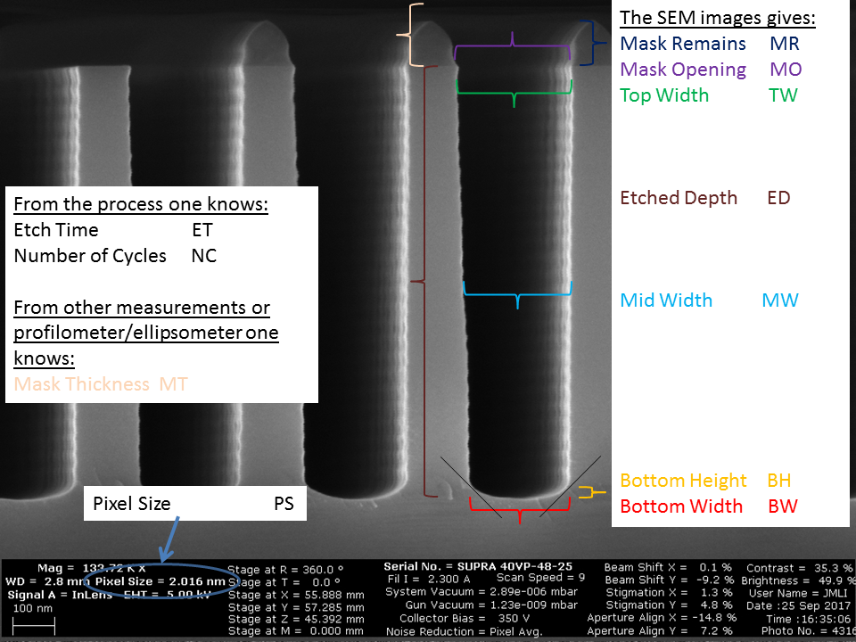
Deep silicon trenches come in many sizes and shapes. The best way of characterizing them is to cleave the wafer perpendicular to the trench and inspect the profile in an SEM or optical microscope. In the SEM the challenge is to get the best information possible about the profile with as little effort as possible. The information acquired must be simple and useful. Below is an example.
Input parameters
Many users make measurements using the annotations in the SEM. However, instead of adding a ton of measurements to each SEM image while at the SEM and hence spend an unreasonable amount of time there, one can postpone making the measurements till afterwards. The only requirement is that the pixel size of every SEM image is known - one can add it to the datazone: See any SEM manual for instructions - for instance HERE
- Opening the images with Irfanview (or any other image viewer with the same possibilities) and drawing squares (the pixel dimensions are shown in the top) as measurements. These squares are one pixel wide compared to the 2 (or even 3) which are default for the annotations in smartSEM.
- Pixel Size (PS)
- Shown in the datazone or read from the tiff header.
- Number of cycles (NC)
- In case of a Bosch process, the number of cycles may be used instead of the process time.
- Etch Time (ET)
- ...self explanatory.
- Mask Thickness (MT)
- The thickness of the mask prior to etching.
- Mask Remains (MR)
- The thickness of the mask after etching.
- Mask Opening (MO)
- The width of the mask opening.
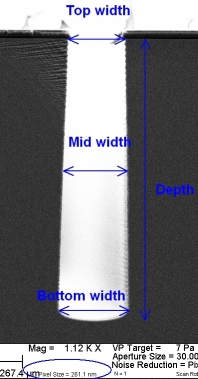
- Top Width (TW)
- The narrowest part of the open feature near the surface.
- Mid Width (MW)
- The width of the trench at half the distance to the bottom of the trench.
- Bottom width (BW)
- The width of the trench at the bottom. As many trenches have more or less rounded corners at the bottom, this point defined to be where the slope passes 45 degrees to the surface as indicated in the SEM image above with black bars.
- Bottom Height (BH)
- The height difference between the 'Bottom width' points and the center of the trench.
- Etched Depth (ED)
- The distance from the top to the bottom of the trench..
- Mask Remains (MR)
- The thickness of the mask that remains.
Output parameters
- Etched depth (nm or µm)
- The etched depth (ED) is rather self explanatory: ED PS
- Etch rate (nm or µm per min.)
- Divide the etched depth (ED) by the etch time (ET) of the process:
- Sidewall bowing (%)
- The sidewall bowing is a measure of how much the sidewall profile deviates from a straight line - regardless of what angle it is at:
- or
- with
- Mask etch rate (nm per min.)
- CD loss (nm per edge)
- Sidewall angle (degrees)
- or
- with
Parameters
Template:Tiny tiny


