Specific Process Knowledge/Characterization/XPS/XPS Depth profiling: Difference between revisions
| Line 10: | Line 10: | ||
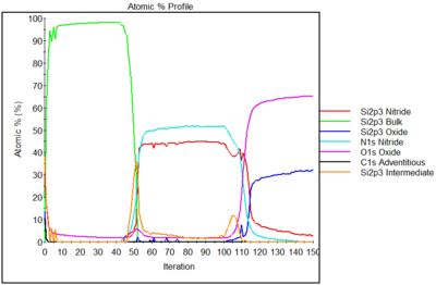
As an example, to the left is shown a depth profile of a sample | As an example, to the left is shown a depth profile of a sample | ||
[[File:profile sandwich 3.PNG|400px]] | |||
As an illustration, a figure to the left, shows an elemental analysis through a metallic film consisting of Ni and Cr. The metallic layer was about 70 nm thick, and the atomic percentage of Ni and Cr was measured through the layer. | As an illustration, a figure to the left, shows an elemental analysis through a metallic film consisting of Ni and Cr. The metallic layer was about 70 nm thick, and the atomic percentage of Ni and Cr was measured through the layer. | ||
In the graph, you see the atomic % as a function of etch depth, and it is possible to detect that the relationship between Ni and Cr is fairly constant through the metallic film. | In the graph, you see the atomic % as a function of etch depth, and it is possible to detect that the relationship between Ni and Cr is fairly constant through the metallic film. | ||
Revision as of 15:25, 14 May 2018
Feedback to this page: click here
Depth profiling
The photoelectrons have a very short inelastic mean free path - this means that although generated at roughly equal numbers from the surface to deep inside the sample, only the photoelectrons emerging from the topmost layers will survive the passage to the surface unscattered. Photoelectrons that have undergone inelastic collisions will have lost a fraction of their kinetic energy - and hence no longer contribute to the intensity of the peak but will find itself in the rise in background signal on the left side of the peak in the spectrum (corresponding to lower kinetic energy).
This means that only atoms sitting in the topmost nanometers of the sample contribute to the intensity of the peak making the technique very surface sensitive. To access deeper layers of the sample one can use the argon ion gun to sputter off the surface layers of the sample - and then record a new set of spectra. A series with cycles of measurement with subsequent sputtering can be set up in this way creating a depth profile of the sample.
Example: NiCr film As an example, to the left is shown a depth profile of a sample

In the graph, you see the atomic % as a function of etch depth, and it is possible to detect that the relationship between Ni and Cr is fairly constant through the metallic film.
