Specific Process Knowledge/Characterization/SEM Jeol: Difference between revisions
| Line 3: | Line 3: | ||
'''Feedback to this page''': '''[mailto:labadviser@danchip.dtu.dk?Subject=Feed%20back%20from%20page%20http://labadviser.danchip.dtu.dk/index.php/Specific_Process_Knowledge/Characterization/SEM_Jeol#SEM_JEOl click here]''' | '''Feedback to this page''': '''[mailto:labadviser@danchip.dtu.dk?Subject=Feed%20back%20from%20page%20http://labadviser.danchip.dtu.dk/index.php/Specific_Process_Knowledge/Characterization/SEM_Jeol#SEM_JEOl click here]''' | ||
=SEM | =SEM JEOL= | ||
[[image:IMG_3290.jpg|400x400px|right|thumb|Picosun R200 ALD, positioned in cleanroom F-2.]] | [[image:IMG_3290.jpg|400x400px|right|thumb|Picosun R200 ALD, positioned in cleanroom F-2.]] | ||
Revision as of 15:30, 9 November 2015
THIS PAGE IS UNDER CONSTRUCTION
Feedback to this page: click here
SEM JEOL

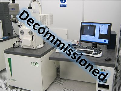
The SEM Jeol is located in the basement of DTU Danchip. I will very soon be decommissioned (within 2015) and replaced and by the SEM Supra 1 (former SEM Zeiss).
The user manual, control instruction, the user APV and contact information can be found in LabManager:
SEM Jeol info page in LabManager,
Performance information
| Equipment | SEM Jeol (Jeol JSM 5500 LV) | |
|---|---|---|
| Purpose | Imaging and measurement of |
|
| Location |
| |
| Performance | Resolution |
The resolution is strongly dependent on the type of sample and the skills of the operator. |
| Instrument specifics | Detectors |
|
| Stage |
| |
| Electron source |
| |
| Operating pressures |
| |
| Substrates | Batch size |
|
| Allowed materials |
| |
