Specific Process Knowledge/Characterization/XPS: Difference between revisions
No edit summary |
|||
| Line 77: | Line 77: | ||
|} | |} | ||
==Carbon Contamination== | ==Carbon Contamination== | ||
--[[User:Kare|kare]] ([[User talk:Kare|talk]]) 09:29, 18 February 2015 (CET) | |||
An unexpected carbon signal is often found in samples during XPS. The carbon typically originates from sample exposure to the air outside the XPS (e.g. the lab). Measurements of carbon contamination of a sputter cleaned Cu sample due to air exposure indicates that carbon contamination builds up to 20 At. % in approximately one minute. | |||
[[File:AirCarbon.jpg]] | |||
Measurements of the At. % of C on the Au-reference in the XPS after an initial sputter clean were conducted for 16 hours every hour. The results show that carbon is detectable after 1-2 hours and gradually builds up at a rate of approximately 0.6 At. percentage points per hour, i.e. much slower than if the sample is exposed to air. Thus carbon contamination on samples in the XPS typically originates from air exposure. | |||
[[File:C-contamination.jpg]] | |||
Revision as of 10:29, 18 February 2015
Feedback to this page: click here
XPS-ThermoScientific

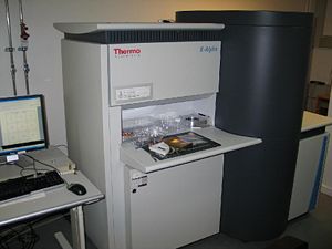
A X-ray Photoelectron Spectroscopy (XPS) system can be used at Danchip. The system is a Thermo K-Alpha system, placed in the basement of building 346.
The user manual(s), user APV(s), technical information and contact information can be found in LabManager:
XPS-ThermoScientific in LabManager
Elemental analysis
The XPS instrument can be used to do elemental analysis, chemical state analysis on the sample surface or deeper down by a depth profiling. A comparison about techniques and instruments used for elemental analysis at Danchip can be found on the page Element analysis.
More about the different possibilities of the XPS instrument is found here:
Equipment performance of XPS-ThermoScientific
| Purpose | Chemical analysis |
|
|---|---|---|
| Performance | Spot size | Can be set between 30µm - 400µm |
| Probing depth | Depending on probed element. Max probe depth lies within 10-200 Å. | |
| Resolution | Dependent on probed elements. Concentrations down to about 0,5 atomic % can in some cases be detected. | |
| Charge compensation |
Flood gun can be used for charge compensation of non conductive samples | |
| Finding structures | Choose measuring spot from camera image (magnified) | |
| Depth profiling | Purpose | With ion beam etch the top layer of the material can be removed, to do a depth profiling |
| Ion beam size | About 3x1 mm | |
| Substrates | Substrate size |
Maximum 60x60 mm |
| Substrate thickness |
Maximum height about 20 mm |
Carbon Contamination
--kare (talk) 09:29, 18 February 2015 (CET)
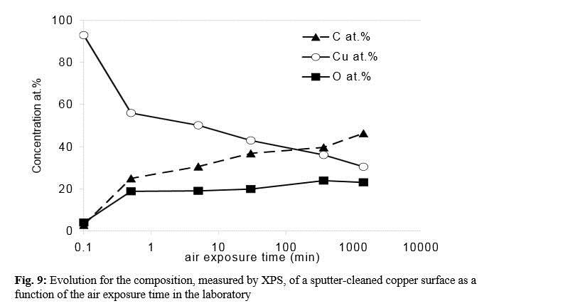
An unexpected carbon signal is often found in samples during XPS. The carbon typically originates from sample exposure to the air outside the XPS (e.g. the lab). Measurements of carbon contamination of a sputter cleaned Cu sample due to air exposure indicates that carbon contamination builds up to 20 At. % in approximately one minute.
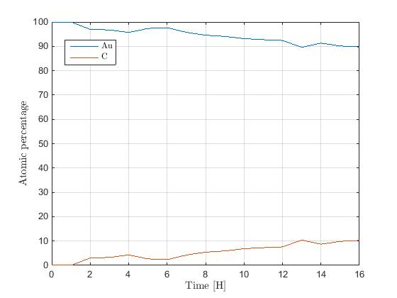
Measurements of the At. % of C on the Au-reference in the XPS after an initial sputter clean were conducted for 16 hours every hour. The results show that carbon is detectable after 1-2 hours and gradually builds up at a rate of approximately 0.6 At. percentage points per hour, i.e. much slower than if the sample is exposed to air. Thus carbon contamination on samples in the XPS typically originates from air exposure.


