Specific Process Knowledge/Etch/IBE⁄IBSD Ionfab 300: Difference between revisions
Appearance
| Line 12: | Line 12: | ||
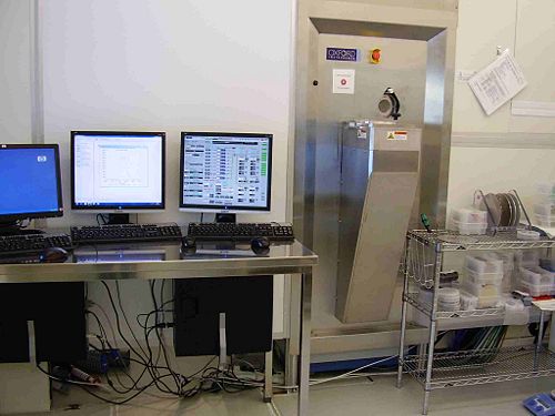
This Ionfab300 from Oxford Instruments is capable of of both ion sputter etching/milling and sputter deposition. | This Ionfab300 from Oxford Instruments is capable of of both ion sputter etching/milling and sputter deposition. | ||
The etching/milling with Argon alone is done by pure physical sputtering of the surface. This causes redeposition on the sidewalls leaving side wall angles at typically between 70-90 degrees (often closest to 70 degrees). | The etching/milling with Argon alone is done by pure physical sputtering of the surface. This causes redeposition on the sidewalls leaving side wall angles at typically between 70-90 degrees (often closest to 70 degrees). | ||
'''The user manual and contact information can be found in LabManager:''' | |||
<!-- remember to remove the type of documents that are not present --> | |||
<!-- give the link to the equipment info page in LabManager: --> | |||
[http://labmanager.danchip.dtu.dk/function.php?module=Machine&view=view&mach=326 IBE/IBSD Ionfab 300+ in LabManager] | |||
==Process information== | ==Process information== | ||
Revision as of 09:03, 21 February 2014
Feedback to this page: click here
IBE/IBSD Ionfab 300: milling, dry etching and deposition in the same tool

IBE: Ion Beam Etch
IBSD: Ion Beam Sputter Deposition
This Ionfab300 from Oxford Instruments is capable of of both ion sputter etching/milling and sputter deposition. The etching/milling with Argon alone is done by pure physical sputtering of the surface. This causes redeposition on the sidewalls leaving side wall angles at typically between 70-90 degrees (often closest to 70 degrees).
The user manual and contact information can be found in LabManager:
IBE/IBSD Ionfab 300+ in LabManager
Process information
Etch
- Some general process trends
- Results from the acceptance test:
- Magnetic stack containing Ta/MnIr/NiFe
- Etch in Stainless steel with X as masking material
- Process develop
Deposition
- Results from the acceptance test:
| Purpose |
|
. |
|---|---|---|
| Performance | Etch rates |
Typical 1-100 nm/min depending om material and process parameters |
| Anisotropy |
| |
| Uniformity |
| |
| Process parameters | Gas flows |
Etch source:
Deposition source:
|
| Substrates | Batch size |
|
| Materials allowed |
| |
| Possible masking material |
|
