Specific Process Knowledge/Etch/ICP Metal Etcher/silicon oxide: Difference between revisions
Appearance
No edit summary |
|||
| Line 1: | Line 1: | ||
===Slow etch of SiO2 with resist as masking material - with | ===Slow etch of SiO2 with resist as masking material - using a 6" carrier wafer with recess === | ||
This recipe can be used for slow etching of SiO2 with resist as masking material | This recipe can be used for slow etching of SiO2 with resist as masking material. Here are some test results presented. | ||
Here are some test results presented. | |||
{| border="2" cellspacing="2" cellpadding="3" | {| border="2" cellspacing="2" cellpadding="3" | ||
Revision as of 14:27, 20 February 2014
Slow etch of SiO2 with resist as masking material - using a 6" carrier wafer with recess
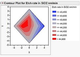
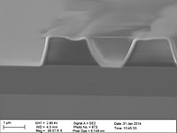
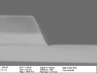
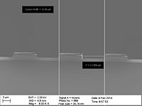
This recipe can be used for slow etching of SiO2 with resist as masking material. Here are some test results presented.
| Parameter | Resist mask |
|---|---|
| Coil Power [W] | 200 |
| Platen Power [W] | 25 |
| Platen temperature [oC] | 0 |
| CF4 flow [sccm] | 20 |
| H2 flow [sccm] | 10 |
| Pressure [mTorr] | 3 |


