Specific Process Knowledge/Thin film deposition/MVD: Difference between revisions
Appearance
No edit summary |
|||
| Line 7: | Line 7: | ||
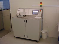
[[image:Mvd.jpg|200x200px|right|thumb|The MVD is located in cleanroom 1]] | [[image:Mvd.jpg|200x200px|right|thumb|The MVD is located in cleanroom 1]] | ||
The Applied Microstructures MVD 100 system deposits molecular films on surfaces. These films serve a wide range of purposes ranging from antistiction coatings of nanoimprint lithography stamps to protecting MEMS structures. At Danchip the MVD is essential for nanoimprint lithography. | The Applied Microstructures MVD 100 system deposits molecular films on surfaces. These films serve a wide range of purposes ranging from antistiction coatings of nanoimprint lithography stamps to protecting MEMS structures. At Danchip the MVD is an essential tool for nanoimprint lithography. | ||
'''The user manual, user APV, and contact information can be found in [http://labmanager.danchip.dtu.dk/function.php?module=Machine&view=view&mach= | '''The user manual, user APV, and contact information can be found in [http://labmanager.danchip.dtu.dk/function.php?module=Machine&view=view&mach=199 LabManager]''' | ||
===Process information=== | ===Process information=== | ||
Revision as of 11:23, 20 January 2014
THIS PAGE IS UNDER CONSTRUCTION
Feedback to this page: click here
The Molecular Vapor Deposition tool

The Applied Microstructures MVD 100 system deposits molecular films on surfaces. These films serve a wide range of purposes ranging from antistiction coatings of nanoimprint lithography stamps to protecting MEMS structures. At Danchip the MVD is an essential tool for nanoimprint lithography.
The user manual, user APV, and contact information can be found in LabManager
Process information
| Purpose |
| ||
|---|---|---|---|
| Resist |
| ||
| Performance | Coating thickness |
| |
| Process parameters | Spin speed |
100 - 5000 rpm | |
| Spin acceleration |
100 - 5000 rpm/s | ||
| Hotplate temperature |
| ||
| Substrates | Substrate size |
| |
| Allowed materials |
All cleanroom materials except III-V materials | ||
| Batch |
1 | ||
