Specific Process Knowledge/Lithography/EBeamLithography/JEOL 9500 User Guide: Difference between revisions
No edit summary |
|||
| (37 intermediate revisions by the same user not shown) | |||
| Line 1: | Line 1: | ||
'''Feedback to this page''': '''[mailto:labadviser@nanolab.dtu.dk?Subject=Feed%20back%20from%20page%20http://labadviser.nanolab.dtu.dk/index.php/Specific_Process_Knowledge/Lithography/EBeamLithography/JEOL 9500 User Guide click here]''' | |||
Content and illustration by Thomas Pedersen, DTU Nanolab unless otherwise noted. | |||
[[File:TPE02803.jpg|right|400px]] | [[File:TPE02803.jpg|right|400px]] | ||
| Line 4: | Line 8: | ||
==Type and location of machine== | ==Type and location of machine== | ||
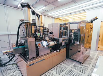
The JEOL JBX-9500FS electron beam lithography system is a spot electron beam lithography system designed for use in writing patterns (10 nm - 1 µm) in electron sensitive resists. The JEOL JBX-9500FS was purchased in 2012 and is installed in E-1 and E-2 at DTU | The JEOL JBX-9500FS electron beam lithography system is a spot electron beam lithography system designed for use in writing patterns (10 nm - 1 µm) in electron sensitive resists. The JEOL JBX-9500FS was purchased in 2012 and is installed in E-1 and E-2 at DTU Nanolab. The main console of the e-beam writer is installed in E-2 which is a class 10 (ISO 4) cleanroom with tight temperature and moisture control. The computer controlling the e-beam (EWS/9500) and the computer supporting the conversion of e-beam files are located in E-1 which is a class 100 (ISO 5) cleanroom. | ||
== | == Training and authorization == | ||
*Only authorized users are allowed to use this machine | *Only authorized users are allowed to use this machine. | ||
*In E-2, all users must keep within the area between the front side of the machine and the table with the pre-aligner setup. Only JEOL staff or DTU Nanolab staff may access the backside of the machine. | *In E-2, all users must keep within the area between the front side of the machine and the table with the pre-aligner setup. Only JEOL staff or DTU Nanolab staff may access the backside of the machine. | ||
*No users, not even authorised users, are allowed to load a | *No users, not even authorised users, are allowed to load a cassette into the automatic cassette transfer system. | ||
*After your exposure, fully trained users can unload their cassettes from the | *After your exposure, fully trained users can unload their cassettes from the automatic cassette transfer system and unmount their substrates. | ||
*If you are | *If you are unable to unmount your substrates before another user requires the cassette, you must accept that either the next user or DTU Nanolab personel unmount your substrates. | ||
*Training can be requested by sending a mail with relevant process flow to training@nanolab.dtu.dk | |||
<br> | |||
== Techical Specification == | |||
The system can be characterized as follows: | |||
*The spot beam for electron beam writing is generated by a ZrO/W emitter and a four-stage electron beam focusing lens system. | |||
*The maximum frequency of the deflector scanner is 200 MHz, i.e. the minimum beam dwell time is 5 ns. | |||
*The acceleration voltage is locked at 100 kV. | |||
*The e-beam writer can pattern structures with a minimum resolution of 10 nm. | |||
*The maximum writing field size is 1000 µm x 1000 µm. | |||
*The machine has cassettes for 2", 4", 6" and 8" wafers and also dedicated cassettes for chips with slot dimensions of 4 mm, 8 mm, 12 mm, and 20 mm. See the [[Specific Process Knowledge/Lithography/EBeamLithography/Cassettes|Cassette specification page for more information.]] | |||
The electromagnetic lens system is illustrated below. | |||
{| style="border: none; border-spacing: 0; margin: 1em auto; text-align: center;" | |||
|- | |||
| [[image:9500Column.png|600px]] | |||
|- | |||
| colspan="1" style="text-align:center;| | |||
Schematic of the JEOL 9500 electromagnetic lens system inside the column. | |||
|} | |||
<br> | <br> | ||
=Job execution= | |||
The following sections describe how a substrate is mounted, transfered to the system and exposed. | |||
==Sample mounting== | |||
The JEOL 9500 system uses a proprietary sample cassette format and thus each sample must be mounted in an appropriate cassette. Cassettes are available for wafer sizes from 2” to 8”. Smaller chips must be mounted in dedicated chip cassettes with slots of four different sizes available. For more information on available cassettes and their specifications please refer to the [[Specific Process Knowledge/Lithography/EBeamLithography/Cassettes|JEOL 9500 cassette specifications page.]] As an example the 4" titanium cassette is shown below. | |||
{| style="border: none; border-spacing: 0; margin: 1em auto; text-align: center;" | |||
|- | |||
| [[image:BSPCL-520.png|1200px]] | |||
|- | |||
| colspan="1" style="text-align:center;| | |||
Back side (left )and front side view (right) of the 4" wafer titanium cassette (BSPCL-520). | |||
|} | |||
If a cassette has been used recently it might be found on the cassette preparation table already, otherwise it will have to be retrieved from the cassette transfer system. This is done from the operation screen of the cassette transfer system. | |||
{| style="border: none; border-spacing: 0; margin: 1em auto; text-align: center;" | |||
|- | |||
| [[image:AutoStocker.png|800px]] | |||
|- | |||
| colspan="2" style="text-align: center;| | |||
Operation screen of the automatic cassette transfer system / auto stocker. | |||
|} | |||
Retrieving a cassette from the automatic cassette transfer system | |||
*Toggle the system to '''Local''' operation mode | |||
*Identify the shelf number for the cassette in question | |||
*Use the '''shelf selector''' to choose that number | |||
*Press the transfer button to transfer it from the shelf to the port/door | |||
*Once the robot is done, click '''Open''' to unlock the door | |||
*Open door, retrieve cassette and place it on a layer of tissues on the cassette preparation table | |||
*Close the door | |||
*Click '''Close''' to lock the door | |||
*Set the system back to '''Remote''' operation | |||
Once the cassette is placed up-side down on the preparation table the slot cover can be removed by pressing down and rotating the spring loaded locking mechanism. The substrate can be placed in the slot using the vacuum tweezer found on the table. As the cassette is up-side down, the substrate must be loaded with resist side down. | |||
{| style="border: none; border-spacing: 0; margin: 1em auto; text-align: center;" | |||
|- | |||
| [[image:TPE02761.jpg|517px]] || [[image:TPE02763.jpg|517px]] | |||
|- | |||
| colspan="2" style="text-align: center;| | |||
Samples can be loaded into appropriate cassettes on the cassette preparation table. | |||
|} | |||
The system is fitted with an auto stocker system that can store 10 cassettes. It is thus possible to prepare multiple substrates and define an automated job to execute exposure of several substrates across several cassettes. After sample loading the cassette must be placed in the automatic cassette transfer system. Users are '''NOT''' allowed to do this. Only Nanolab staff who are members of the E-beam Loading Team may place cassettes into the automatic cassette transfer system. Hence users must always contact the Nanolab E-beam loading team prior to exposure to have their cassette loaded into the cassette transfer system. The E-beam loading team can be contacted at [email]. Upon loading a cassette Nanolab staff will visually verify the sample has been installed and secured correctly. Incorrect sample mounting can lead to severe damage to the internal parts of the JEOL 9500 exposure system. | |||
<div class="center" style="color:red; width:auto; margin-left:auto; margin-right:auto;">'''Any user found to load cassettes to the cassette transfer system themselves will be permanently excluded from using the JEOL 9500 system.'''</div> | |||
{| style="border: none; border-spacing: 0; margin: 1em auto; text-align: center;" | |||
|- | |||
| [[image:TPE02777.jpg|300px]] | |||
|- | |||
| colspan="1" style="text-align:center;| | |||
Nanolab staff member loading the 4" wafer cassette to the automatic cassette transfer system. | |||
|} | |||
General rules for handling cassettes and mounting wafers and chips into cassettes: | |||
*Always wear face-mask and a new pair of gloves | |||
*Never put cassettes directly on the table, use lint-free cleanroom tissues | |||
*Never touch the reference planes, i.e. the six polished areas on the front side of the cassette | |||
*Never lift the cassette in the hook | |||
*Always check the wafer for loose parts or flakes before loading. In case of loose parts or flakes, stop mounting, discard or rework the sample and rethink your process. | |||
*Always check the cassette for loose parts, dust and particles. | |||
*When exposing chips, make sure the chip size is at least 2 mm larger than the slot opening. Be careful when mounting the cover plate, it will get stuck easily if mounted at a slight tilt. '''Never push the cover into place,''' it must fall in by itself. | |||
*When mounting a wafer, hold the spring (wafer securing pin) back when putting the wafer and the cover into the cassette, especially on the 2" cassette (the spring can lift the wafer). Tighten the leaf spring first, then release the spring and tighten the rotation lock lever. | |||
*Inspect the front side of the cassette carefully after mounting the chip/wafer; a small gap between substrate and cassette will lead to a failure in HEIMAP and no exposure is thus possible. | |||
<br> | <br> | ||
== | ==Cassette transfer== | ||
Cassette transfer is controlled from the '''Loader''' program. If it is not open it can be opened from the '''EBX Menu''' by clicking '''Ldr.''' | |||
{| style="border: none; border-spacing: 0; margin: 1em auto; text-align: center;" | |||
|- | |||
| [[image:EBXMenu.png|500px]] | |||
|- | |||
| colspan="1" style="text-align:center;| | |||
All essential programs can be started from the EBX Menu. | |||
|} | |||
{| style="border: none; border-spacing: 0; margin: 1em auto; text-align: center;" | |||
|- | |||
| [[image:EBLLoader.png|600px]] | |||
|- | |||
| colspan="1" style="text-align:center;| | |||
The Loader window controls cassette exchange between the writing system and the cassette transfer system. | |||
|} | |||
The '''Loader''' window shows available cassettes in the automatic transfer system and which cassette is currently inside the writing system. In this example cassette 10 is inside the writing system. Cassettes can be moved between the writing system and the transfer system with the '''Carry in''' and '''Carry out''' buttons. '''Carry in''' will move the selected cassette to the writing system while '''Carry out''' will move the selected cassette to the selected shelf in the transfer system. In order to move a particular cassette into the writing system the current cassette must naturally be moved out first. | |||
The '''EXCH EVAC''' switch must always be left unchecked as in this example. If it is toggled on the exchange chamber (load lock) will be pumped down after a carry out operation and the next carry in operation must then wait for the pump down (15 min) before it can be executed. Always leave '''EXCH EVAC''' off. | |||
Prior to exposure the chosen cassette has to be transferred from the cassette transfer system and to the main chamber. This is done from the “Loader” module by first moving out the current cassette from the main chamber and then moving in the cassette used for exposure. Carry out takes about 4 minutes while carry in takes about 15 min since the exchange chamber has to pump down to vacuum. The procedure is | |||
*Make sure '''EXCH EVAC''' is toggled off | |||
*Press '''Carry out''' to move the current cassette back to the shelf it was loaded from | |||
*After about 4 min the status light will be solid green, select the cassette to use | |||
*Press '''Carry in''' | |||
*The system will be ready after about 15 min | |||
<br> | <br> | ||
==System calibration== | |||
After cassette transfer the system has to be calibrated with the chosen beam current condition profile. This is done in a mostly automated sequence with only minute input from the user. The sequence is explained in detail in the following but in overview it is | |||
*Select and restore the system to the chosen beam current profile | |||
*System self check | |||
**Execute a current measurement | |||
**Execute absorbed electron mark detection | |||
**Execute backscatter electron mark detection | |||
*Execute self calibration routine '''daily''' | |||
*Verify drift is low | |||
*Map height profile of sample | |||
*Save data into calibration profile | |||
*Execute pattern writing | |||
===Select and restore the system to the chosen beam current profile=== | |||
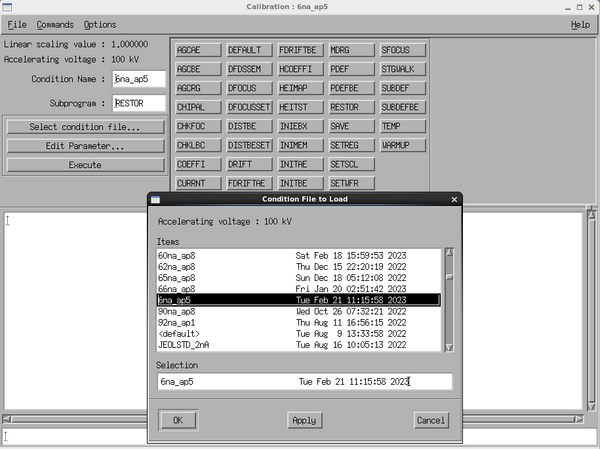
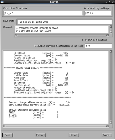
The SDF specifies which system condition file to use for the exposure, this determines the beam current. Condition files are named according to beam current and beam aperture, for instance '''6nA_ap5''' which will expose at 6 nA using aperture 5. Restoring a condition file for use is done from the '''Calibration''' window, if it is not open it can be opened from the '''EBX Menu'''. | |||
*Select the '''RESTOR''' subprogram in the '''Calibration''' window | |||
*Click '''Select condition file...''' | |||
*Browse and select the condition file to use and click '''OK''' | |||
*Click '''Edit parameter...''' | |||
*Click '''Execute''' in the '''RESTOR''' window | |||
The bottom line of the '''Calibration''' window will now display ''Received an intermediate result RESTOR(DEMAG)'' to indicate it is working. Setting up for the new condition file takes about 1 minute and the bottom line will say ''Finished subprogram RESTOR'' when done. | |||
{| style="border: none; border-spacing: 0; margin: 1em auto; text-align: center;" | |||
|- | |||
| [[image:9500calib1.png|600px]] || [[image:9500restor1.png|400px]] | |||
|- | |||
| colspan="2" style="text-align:center;| | |||
'''Calibration''' and '''RESTOR''' windows. | |||
|} | |||
===System self calibration=== | |||
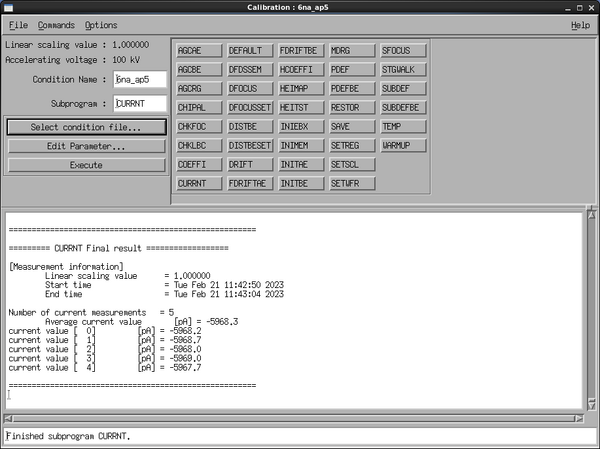
With the correct condition file restored the next step is to measure beam current and verify that it is close to the expected value. | |||
*Select the '''Current''' subprogram and click '''Execute''' in the '''Calibration''' window | |||
The stage moves to the faraday cup to measure beam current. This takes 15 seconds and the '''Calibration''' window will display the measured beam current. Note this down for the Labmanager usage log. If the value is more than 5% off the expected beam current call the e-beam responsible for assistance. | |||
{| style="border: none; border-spacing: 0; margin: 1em auto; text-align: center;" | |||
|- | |||
| [[image:9500current1.png|600px]] | |||
|- | |||
| colspan="1" style="text-align:center;| | |||
Result display of current measurement. | |||
|} | |||
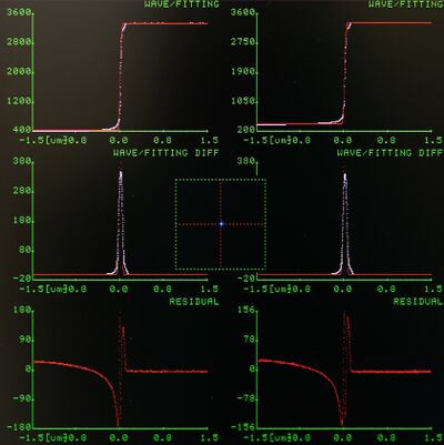
The next self check is to see if the machine can find the Absorbed Electron (AE) mark and the Backscatter Electron (BE) mark. The procedure is | |||
*Select the '''INITAE''' subprogram and click '''Execute''' | |||
*Verify that the graph in the SSP window shows the characteristic step function centered at 0 on the x-axis | |||
*Select the '''INITBE''' subprogram and click '''Execute''' | |||
*Verify that the graph in the SSP window shows the characteristic step function centered at 0 on the x-axis | |||
{| style="border: none; border-spacing: 0; margin: 1em auto; text-align: center;" | |||
|- | |||
| [[image:JEOLSSP1.jpg|400px]] || [[image:JEOLSSP2.jpg|400px]] | |||
|- | |||
| colspan="2" style="text-align:center;| | |||
Correct result of '''INITAE''' (left) and '''INITBE''' (right). | |||
|} | |||
Correct execution will look like above. '''INITAE''' uses the beam to scan a PN-junction which the system uses to determine beam position and shape. '''INITBE''' uses the beam to scan a gold marker on the stage which the system uses for position and distortion correction of the beam placement within the writing field. The top row shows the signal, the following rows shows the 1st and 2nd derivative, respectively. | |||
=== Auto calibration === | |||
The system can auto calibrate itself using the AE and BE stage marks. The system will automatically measure beam position at various locations of the writing field to determine position errors. A correction matrix will be applied and the beam position will be remeasured to validate the result. The sequence takes about 8 minutes to execute. This should be done every time beam current is changed, i.e. a new condition file is restored. The procedure is | |||
*From the '''Calibration''' window choose '''Commands''' at the top of the window and click '''Batch''' | |||
*From the '''BATCH parameter''' window click '''Condition file...''' | |||
*Browse for the '''daily''' file and click '''OK''' | |||
*Click '''Execute''' | |||
{| style="border: none; border-spacing: 0; margin: 1em auto; text-align: center;" | |||
|- | |||
| [[image:9500dayli1.png|600px]] | |||
|- | |||
| colspan="1" style="text-align:center;| | |||
Load the '''daily''' batch command and execute it. | |||
|} | |||
During calibration the system will measure and display the beam position at 49 locations of the writing field. The position error (in nm) can be read of the matrices during execution, an example is shown below. At the end of the process the '''Calibration''' window will display '''Finished BATCH CALIB'''. | |||
{| style="border: none; border-spacing: 0; margin: 1em auto; text-align: center;" | |||
|- | |||
| [[image:9500dist1.png|600px]] | |||
|- | |||
| colspan="1" style="text-align:center;| | |||
Example of beam offset matrix shown during auto calibration. Average beam offset is below 1 nm within the 1000 x 1000 µm<sup>2</sup> writing field in this example. Image: Thomas Pedersen. | |||
|} | |||
===Measure stage drift=== | |||
The next step is to measure stage drift. This is done from the '''Calibration''' window. | |||
*Select the '''Drift''' subprogram and click '''Execute''' | |||
The system will scan the drift mark (BE mark) to determine drift since last drift reset. The absolute value is not important since it is unknown when the drift subprogram was last reset. The time variation of the drift measurements is however important thus one should compare two drift measurements taken 1-2 minutes apart. Luckily the '''dayli''' batch command ended with a drift measurement, having made one manually we can now compare the result, see the example below. | |||
{| style="border: none; border-spacing: 0; margin: 1em auto; text-align: center;" | |||
|- | |||
| [[image:9500drift1.png|600px]] | |||
|- | |||
| colspan="1" style="text-align:center;| | |||
Comparison of two drift measurements. | |||
|} | |||
In this example the two drift measurements are made a bit more than 1 minute apart (look at timestamps). The x-axis drift has changed from 65.4 nm to 64.2 nm, i.e. a change of 1.2 nm in about 1 minute. The y-axis drift has changed from 85.3 nm to 86.8 nm, a shift of 1.5 nm in about 1 minute. Thus the drift is about 1-1.5 nm/min in this particular example. This is a typical value. If you experience drift of 5-10 nm/min, give the system 10 min to thermally equilibrate and try again. If drift is above 10 nm/min please call the e-beam personnel for assistance. | |||
===Measure height profile of sample=== | |||
The height of the sample surface must be known to focus the electron beam properly at the surface. This can be done using the '''HEIMAP''' subprogram. | |||
*Select on the '''HEIMAP''' subprogram in the '''Calibration''' window | |||
*Click '''Edit Parameter...''' | |||
*This opens the '''HEIMAP''' parameters window, make sure to edit the following parameters | |||
**Check '''Wafer''' and not '''Mask''' | |||
**Choose correct '''Material size''' in the dropdown | |||
**Choose the correct slot ID in '''Multi-piece window''' | |||
**Set a reasonable number in x and y '''Number of height measurement points''' | |||
**Set a reasonable x- and y-axis pitch in the '''Height data measurement pitch''' fields | |||
**Set '''Offset''' fields to zero | |||
*Click '''Save''' in order to save the setup for execution during exposure | |||
*Click '''Execute''' to execute and verify result | |||
{| style="border: none; border-spacing: 0; margin: 1em auto; text-align: center;" | |||
|- | |||
| [[image:9500heimap1.png|500px]] | |||
|- | |||
| colspan="1" style="text-align:center;| | |||
Parameter window of the '''HEIMAP''' subprogram. | |||
|} | |||
The example above will create a 3x3 matrix of height data with a pitch of 1 mm in x and y. After execution the system will display a matrix with height measurement data in µm. Verify that there are no outliers and that variation is less than 100 µm from top to bottom. | |||
===Save condition file=== | |||
For the calibration data to have effect during exposure the data must be saved into the calibration profile. This is done via the '''SAVE''' subprogram from the '''Calibration''' window. | |||
*Select the '''SAVE''' subprogram | |||
*Click '''Edit Parameter...''' | |||
*From the '''SAVE''' window click '''Acquisition of latest status''' | |||
*Wait 5 seconds for the window to populate with data | |||
*Click '''Apply''' and '''Save''' | |||
{| style="border: none; border-spacing: 0; margin: 1em auto; text-align: center;" | |||
|- | |||
| [[image:9500save1.png|500px]] | |||
|- | |||
| colspan="1" style="text-align:center;| | |||
Acquire the calibration data and then apply the data to save. | |||
|} | |||
All of the calibration data is now saved and the system is ready for exposure. | |||
===Job execution=== | |||
The job and the system is now ready to execute the exposure. | |||
*Open the '''Expose''' program from the '''EBX Menu''' | |||
*In the '''Expose''' program click '''File''' and '''Magazine File...''' | |||
*Browse for and select the correct file and click '''OK''' | |||
*The '''Expose''' window is now updated with the file loaded into the '''Magazine filename:''' field | |||
*Click '''Execute''' | |||
*This opens the '''Pattern writing execution check''' window where one can check that the cassette number execution time is as expected before hitting '''Yes''' | |||
{| style="border: none; border-spacing: 0; margin: 1em auto; text-align: center;" | |||
|- | |||
| [[image:9500exposure1.png|500px]] | |||
|- | |||
| colspan="1" style="text-align:center;| | |||
'''Expose''' window with .mgn file loaded for exposure. Notice that the '''Progress''' part of the window still shows the previous exposure information. This field will not update until exposure is started. | |||
|} | |||
{| style="border: none; border-spacing: 0; margin: 1em auto; text-align: center;" | |||
|- | |||
| [[image:9500expose2.png|400px]] | |||
|- | |||
| colspan="1" style="text-align:center;| | |||
Use the '''Pattern writing execution check''' window to verify the cassette number and estimated execution time. Image: Thomas Pedersen. | |||
|} | |||
The system will now carry out initial and cyclic calibration as defined by the path in the JDF file and then exposure will start. The pattern writing can be observed in the SSP window (top left) once it starts. Progress can be monitored in the '''Expose''' window which will give a completion percentage and completion time for the current sequence. Once exposure is completed the system will confirm this with the '''Pattern writing completed''' window. | |||
<br> | <br> | ||
== | = Table of important subprograms = | ||
Below is a brief explanation of some of the most important subprograms found in the '''Calibration''' window. The subprograms listed in the blue part of the table are a part of the 'daily' batch of programs. | |||
{|border="1" cellspacing="0" cellpadding="3" style="text-align:left;" style="width: 75%" | |||
|- | |||
|- | |||
|-style="background:Black; color:White" | |||
!colspan="2"|Calibration of condition files | |||
|- | |||
|- | |||
|-style="background:WhiteSmoke; color:black" | |||
!style="width: 25%"|Subprogram | |||
!Explanation | |||
|- | |||
The | |- | ||
|-style="background:WhiteSmoke; color:black" | |||
!style="background:#ADD8E6; color:Black"|CURRNT | |||
|The stage moves the Faraday's cup to the beam and the machine reads the value of the cup. The machine measures the beam current 5 times and calculate the average of the beam current based on these 5 measurements. | |||
|- | |||
|- | |||
|-style="background:WhiteSmoke; color:black" | |||
!style="background:#ADD8E6; color:Black"|INITAE | |||
|The AE marks (Absorbed Electrons) is a mark type that is connected to a pn-junction, i.e. the current abosrbed in the mark is measured. The AE mark is a knife-edge mark, i.e. is has (originally) very sharp edges. When the beam (with a well-known frequency) scans over this type of mark and absorbed current simultanously is measured, an estimate of the beam diameter can be found. '''INITAE''' is a subprogram that finds the AE mark and scans it for testing that the machine can find the mark. | |||
|- | |||
|- | |||
|-style="background:WhiteSmoke; color:black" | |||
!style="background:#ADD8E6; color:Black"|INITBE | |||
|The BE mark (Backscattered Electrons) is a mark type that consists of a suspended grid of metal. The openings in the grid is 500 microns in both X and Y. When the beam scans over this type of mark, backscattered electrons are detected with the BE detector inside the chamber. This type of mark is used to correlate stage position and beam position during calibration. '''INITBE''' is a subprogram that find the BE mark and scans it for testing that the machine can find the mark. | |||
|- | |||
= | |- | ||
|-style="background:WhiteSmoke; color:black" | |||
!style="background:#ADD8E6; color:Black"|[[Specific_Process_Knowledge/Lithography/EBeamLithography/JBX9500Manual#SFOCUS|SFOCUS]] | |||
|This subprogram finds the minimum beam diameter by scanning an AE mark while changing the focus of the objective lens. The objective lens is defined to be in focus where the machine finds the minimum beam diameter. This program can also be used to observe the depth of focus of a certain condition file. '''The SFOCUS''' subprogram does not work well for currents above 6 nA, why SFOCUS is deleted in 'daily' routines of condition files with currents larger than 6 nA. | |||
|- | |||
|- | |||
|-style="background:WhiteSmoke; color:black" | |||
!style="background:#ADD8E6; color:Black"|[[Specific_Process_Knowledge/Lithography/EBeamLithography/JBX9500Manual#PDEFBE|PDEFBE]] | |||
|Using a BE mark, this subprogram corrects deflection gain and rotation of the main deflector. The system positions the BE mark in the corners of the main field (which is a 1000 x 1000 µm2 square) and scans the mark using the primary deflector only. | |||
|- | |||
|- | |||
|-style="background:WhiteSmoke; color:black" | |||
!style="background:#ADD8E6; color:Black"|[[Specific_Process_Knowledge/Lithography/EBeamLithography/JBX9500Manual#DISTMEM_and_DISTBE|DISTMEM]] | |||
|This subprogram measures the distortion of the beam deflection 7 x 7 positions within the main writing field and generates a distortion correction table. The system positions the BE mark in all 49 positions and uses only the primary deflector to scan the BE mark in every 49 positions. The program sets the distortion directly below the beam (center of the field) to zero. The distortion correction memory in every position in the main writing field is generated by a linear approximation based on the 7 x 7 table. For 0.2 nA or 2 nA, a reasonable convergence value is e.g. 6 nm. | |||
|- | |||
The | |- | ||
|-style="background:WhiteSmoke; color:black" | |||
!style="background:#ADD8E6; color:Black"|[[Specific_Process_Knowledge/Lithography/EBeamLithography/JBX9500Manual#DISTMEM_and_DISTBE|DISTBE]] | |||
|This subprogram measures the distortion of the beam deflection 7 x 7 positions within the main writing field and generates a distortion correction table. The system positions the BE mark in all 49 positions and uses only the primary deflector to scan the BE mark in every 49 positions. The program sets the distortion directly below the beam (center of the field) to zero. The distortion correction memory in every position in the main writing field is generated by a cubic approximation based on the 7 x 7 table. For 0.2 nA or 2 nA, a reasonable convergence value is e.g. 8 nm. | |||
|- | |||
|- | |||
|-style="background:WhiteSmoke; color:black" | |||
!style="background:#ADD8E6; color:Black"|[[Specific_Process_Knowledge/Lithography/EBeamLithography/JBX9500Manual#SUBDEFBE|SUBDEFBE]] | |||
|Using a BE mark, this subprogram corrects deflection gain and rotation of the secondary (sub) deflector. The system positions the BE mark in the corners of the subfield (which is a 4 x 4 µm2 square) and scans the mark using the sub deflector only. | |||
|- | |||
|- | |||
|-style="background:WhiteSmoke; color:black" | |||
![[Specific_Process_Knowledge/Lithography/EBeamLithography/JBX9500Manual#DRIFT|DRIFT]] | |||
|This subprograms scans the DRIFT mark. The DRIFT mark can either be a BE mark or an alignment mark on the substrate. By scanning the DRIFT mark during exposure, the machine can positionally adjust the exposed pattern during writing, i.e. positional drift due to cassette heat-up or warm-up during writing can be corrected. This is done by using the the path DRF5M in the jdf-file. | |||
|- | |||
|- | |||
|-style="background:WhiteSmoke; color:black" | |||
![[Specific_Process_Knowledge/Lithography/EBeamLithography/JBX9500Manual#HEIMAP|HEIMAP]] | |||
|This subprogram measures the height of the substrate to be exposed. The size and workpiece position of the substrate (e.g. 4B) should be entered along with information of desired area to measure height. This area should always be larger than the area of the exposed pattern. The system will focus the beam to the average of the height mesaured in HEIMAP, but '''only''' if you expose in mask writing mode (i.e. no aligning) and execute HEIMAP in your initial calibration (e.g. by using path DRF5M). | |||
|- | |||
|- | |||
|-style="background:WhiteSmoke; color:black" | |||
![[Specific_Process_Knowledge/Lithography/EBeamLithography/JBX9500Manual#SETWFR|SETWFR]] | |||
|This subprograms scans the global marks of the substrate. You need to enter the theoretical positions of the global marks (in wafer coordinate system) and the offset found during pre-aligning. When SETWFR has succeeded in finding your global marks, it will give you a corrected offset, that should be entered in your sdf-file. | |||
|- | |||
|- | |||
! | |-style="background:WhiteSmoke; color:black" | ||
![[Specific_Process_Knowledge/Lithography/EBeamLithography/JBX9500Manual#CHIPAL|CHIPAL]] | |||
|This subprogram scan a set of chip marks on the substrate. You need to enter theoretical position of a chip on your wafer (in wafer coordinate systems) and the theoretical positions of the chip marks on that chip (in chip coordinate system). CHIPAL will then scan 1 or 4 chip marks (mode 1 or mode 4). | |||
| | |- | ||
| | |||
|} | |||
<br> | |||
=Job execution with alignment= | |||
Execution of jobs that require alignment requires a few additional steps compared to the process described above. The additional steps are: | |||
*Optical prealignment of the mounted substrate to determine PQ mark offsets and substrate rotation | |||
*Gain correction to ensure the backscatter detector provides sufficient signal for mark detection using '''AGCRG''' | |||
*Verification of PQ mark detection using '''SETWFR''' | |||
*Verification of chip mark detection using '''CHIPAL''' if chip marks are used | |||
Latest revision as of 11:41, 22 April 2024
Feedback to this page: 9500 User Guide click here
Content and illustration by Thomas Pedersen, DTU Nanolab unless otherwise noted.
Purpose, location and technical specifications
Type and location of machine
The JEOL JBX-9500FS electron beam lithography system is a spot electron beam lithography system designed for use in writing patterns (10 nm - 1 µm) in electron sensitive resists. The JEOL JBX-9500FS was purchased in 2012 and is installed in E-1 and E-2 at DTU Nanolab. The main console of the e-beam writer is installed in E-2 which is a class 10 (ISO 4) cleanroom with tight temperature and moisture control. The computer controlling the e-beam (EWS/9500) and the computer supporting the conversion of e-beam files are located in E-1 which is a class 100 (ISO 5) cleanroom.
Training and authorization
- Only authorized users are allowed to use this machine.
- In E-2, all users must keep within the area between the front side of the machine and the table with the pre-aligner setup. Only JEOL staff or DTU Nanolab staff may access the backside of the machine.
- No users, not even authorised users, are allowed to load a cassette into the automatic cassette transfer system.
- After your exposure, fully trained users can unload their cassettes from the automatic cassette transfer system and unmount their substrates.
- If you are unable to unmount your substrates before another user requires the cassette, you must accept that either the next user or DTU Nanolab personel unmount your substrates.
- Training can be requested by sending a mail with relevant process flow to training@nanolab.dtu.dk
Techical Specification
The system can be characterized as follows:
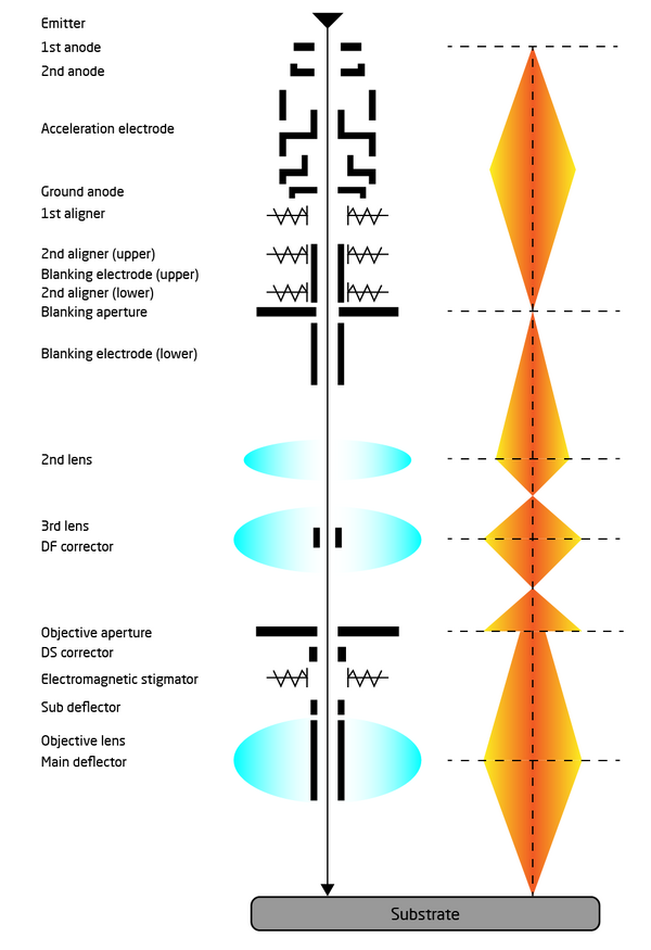
- The spot beam for electron beam writing is generated by a ZrO/W emitter and a four-stage electron beam focusing lens system.
- The maximum frequency of the deflector scanner is 200 MHz, i.e. the minimum beam dwell time is 5 ns.
- The acceleration voltage is locked at 100 kV.
- The e-beam writer can pattern structures with a minimum resolution of 10 nm.
- The maximum writing field size is 1000 µm x 1000 µm.
- The machine has cassettes for 2", 4", 6" and 8" wafers and also dedicated cassettes for chips with slot dimensions of 4 mm, 8 mm, 12 mm, and 20 mm. See the Cassette specification page for more information.
The electromagnetic lens system is illustrated below.
|
|
Schematic of the JEOL 9500 electromagnetic lens system inside the column. |
Job execution
The following sections describe how a substrate is mounted, transfered to the system and exposed.
Sample mounting
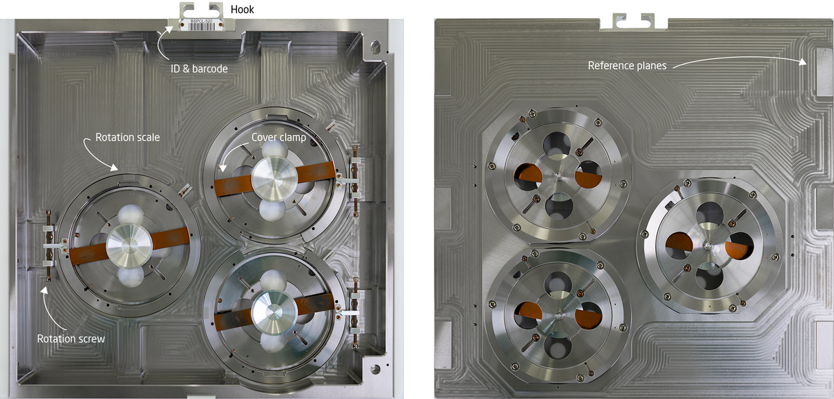
The JEOL 9500 system uses a proprietary sample cassette format and thus each sample must be mounted in an appropriate cassette. Cassettes are available for wafer sizes from 2” to 8”. Smaller chips must be mounted in dedicated chip cassettes with slots of four different sizes available. For more information on available cassettes and their specifications please refer to the JEOL 9500 cassette specifications page. As an example the 4" titanium cassette is shown below.
|
|
Back side (left )and front side view (right) of the 4" wafer titanium cassette (BSPCL-520). |
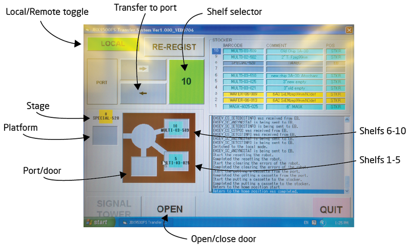
If a cassette has been used recently it might be found on the cassette preparation table already, otherwise it will have to be retrieved from the cassette transfer system. This is done from the operation screen of the cassette transfer system.
| |
|
Operation screen of the automatic cassette transfer system / auto stocker. | |
Retrieving a cassette from the automatic cassette transfer system
- Toggle the system to Local operation mode
- Identify the shelf number for the cassette in question
- Use the shelf selector to choose that number
- Press the transfer button to transfer it from the shelf to the port/door
- Once the robot is done, click Open to unlock the door
- Open door, retrieve cassette and place it on a layer of tissues on the cassette preparation table
- Close the door
- Click Close to lock the door
- Set the system back to Remote operation
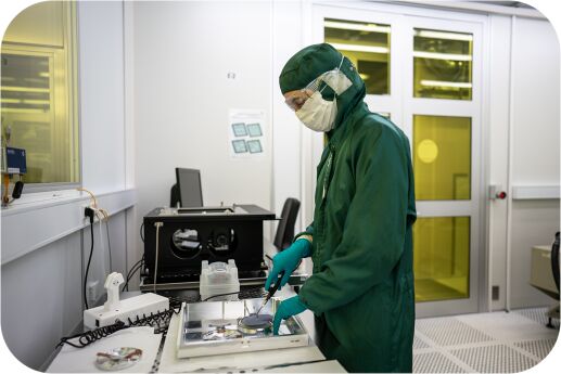
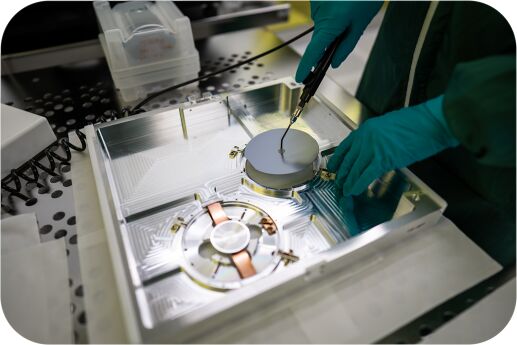
Once the cassette is placed up-side down on the preparation table the slot cover can be removed by pressing down and rotating the spring loaded locking mechanism. The substrate can be placed in the slot using the vacuum tweezer found on the table. As the cassette is up-side down, the substrate must be loaded with resist side down.
 |
|
|
Samples can be loaded into appropriate cassettes on the cassette preparation table. | |
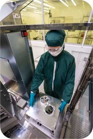
The system is fitted with an auto stocker system that can store 10 cassettes. It is thus possible to prepare multiple substrates and define an automated job to execute exposure of several substrates across several cassettes. After sample loading the cassette must be placed in the automatic cassette transfer system. Users are NOT allowed to do this. Only Nanolab staff who are members of the E-beam Loading Team may place cassettes into the automatic cassette transfer system. Hence users must always contact the Nanolab E-beam loading team prior to exposure to have their cassette loaded into the cassette transfer system. The E-beam loading team can be contacted at [email]. Upon loading a cassette Nanolab staff will visually verify the sample has been installed and secured correctly. Incorrect sample mounting can lead to severe damage to the internal parts of the JEOL 9500 exposure system.
|
|
Nanolab staff member loading the 4" wafer cassette to the automatic cassette transfer system. |
General rules for handling cassettes and mounting wafers and chips into cassettes:
- Always wear face-mask and a new pair of gloves
- Never put cassettes directly on the table, use lint-free cleanroom tissues
- Never touch the reference planes, i.e. the six polished areas on the front side of the cassette
- Never lift the cassette in the hook
- Always check the wafer for loose parts or flakes before loading. In case of loose parts or flakes, stop mounting, discard or rework the sample and rethink your process.
- Always check the cassette for loose parts, dust and particles.
- When exposing chips, make sure the chip size is at least 2 mm larger than the slot opening. Be careful when mounting the cover plate, it will get stuck easily if mounted at a slight tilt. Never push the cover into place, it must fall in by itself.
- When mounting a wafer, hold the spring (wafer securing pin) back when putting the wafer and the cover into the cassette, especially on the 2" cassette (the spring can lift the wafer). Tighten the leaf spring first, then release the spring and tighten the rotation lock lever.
- Inspect the front side of the cassette carefully after mounting the chip/wafer; a small gap between substrate and cassette will lead to a failure in HEIMAP and no exposure is thus possible.
Cassette transfer
Cassette transfer is controlled from the Loader program. If it is not open it can be opened from the EBX Menu by clicking Ldr.

|
|
All essential programs can be started from the EBX Menu. |
|
|
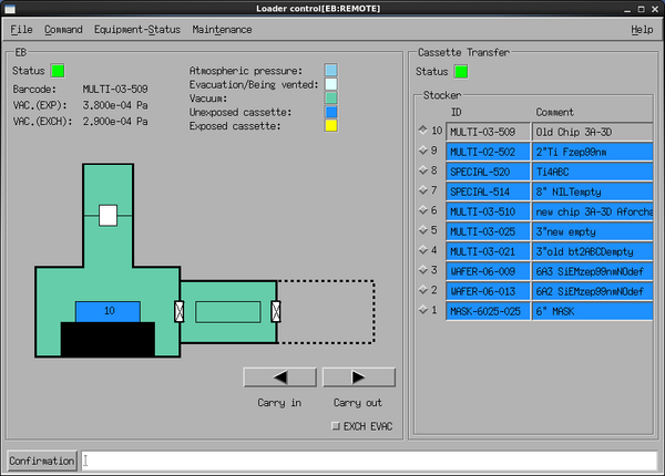
The Loader window controls cassette exchange between the writing system and the cassette transfer system. |
The Loader window shows available cassettes in the automatic transfer system and which cassette is currently inside the writing system. In this example cassette 10 is inside the writing system. Cassettes can be moved between the writing system and the transfer system with the Carry in and Carry out buttons. Carry in will move the selected cassette to the writing system while Carry out will move the selected cassette to the selected shelf in the transfer system. In order to move a particular cassette into the writing system the current cassette must naturally be moved out first.
The EXCH EVAC switch must always be left unchecked as in this example. If it is toggled on the exchange chamber (load lock) will be pumped down after a carry out operation and the next carry in operation must then wait for the pump down (15 min) before it can be executed. Always leave EXCH EVAC off.
Prior to exposure the chosen cassette has to be transferred from the cassette transfer system and to the main chamber. This is done from the “Loader” module by first moving out the current cassette from the main chamber and then moving in the cassette used for exposure. Carry out takes about 4 minutes while carry in takes about 15 min since the exchange chamber has to pump down to vacuum. The procedure is
- Make sure EXCH EVAC is toggled off
- Press Carry out to move the current cassette back to the shelf it was loaded from
- After about 4 min the status light will be solid green, select the cassette to use
- Press Carry in
- The system will be ready after about 15 min
System calibration
After cassette transfer the system has to be calibrated with the chosen beam current condition profile. This is done in a mostly automated sequence with only minute input from the user. The sequence is explained in detail in the following but in overview it is
- Select and restore the system to the chosen beam current profile
- System self check
- Execute a current measurement
- Execute absorbed electron mark detection
- Execute backscatter electron mark detection
- Execute self calibration routine daily
- Verify drift is low
- Map height profile of sample
- Save data into calibration profile
- Execute pattern writing
Select and restore the system to the chosen beam current profile
The SDF specifies which system condition file to use for the exposure, this determines the beam current. Condition files are named according to beam current and beam aperture, for instance 6nA_ap5 which will expose at 6 nA using aperture 5. Restoring a condition file for use is done from the Calibration window, if it is not open it can be opened from the EBX Menu.
- Select the RESTOR subprogram in the Calibration window
- Click Select condition file...
- Browse and select the condition file to use and click OK
- Click Edit parameter...
- Click Execute in the RESTOR window
The bottom line of the Calibration window will now display Received an intermediate result RESTOR(DEMAG) to indicate it is working. Setting up for the new condition file takes about 1 minute and the bottom line will say Finished subprogram RESTOR when done.
 |
|
|
Calibration and RESTOR windows. | |
System self calibration
With the correct condition file restored the next step is to measure beam current and verify that it is close to the expected value.
- Select the Current subprogram and click Execute in the Calibration window
The stage moves to the faraday cup to measure beam current. This takes 15 seconds and the Calibration window will display the measured beam current. Note this down for the Labmanager usage log. If the value is more than 5% off the expected beam current call the e-beam responsible for assistance.
|
|
Result display of current measurement. |
The next self check is to see if the machine can find the Absorbed Electron (AE) mark and the Backscatter Electron (BE) mark. The procedure is
- Select the INITAE subprogram and click Execute
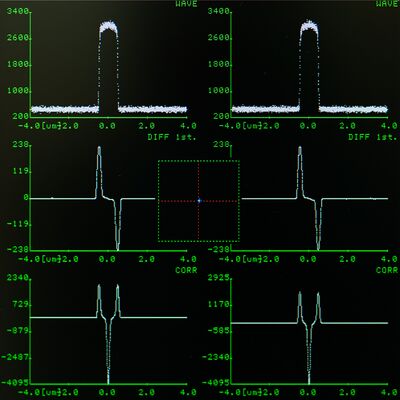
- Verify that the graph in the SSP window shows the characteristic step function centered at 0 on the x-axis
- Select the INITBE subprogram and click Execute
- Verify that the graph in the SSP window shows the characteristic step function centered at 0 on the x-axis
 |
|
|
Correct result of INITAE (left) and INITBE (right). | |
Correct execution will look like above. INITAE uses the beam to scan a PN-junction which the system uses to determine beam position and shape. INITBE uses the beam to scan a gold marker on the stage which the system uses for position and distortion correction of the beam placement within the writing field. The top row shows the signal, the following rows shows the 1st and 2nd derivative, respectively.
Auto calibration
The system can auto calibrate itself using the AE and BE stage marks. The system will automatically measure beam position at various locations of the writing field to determine position errors. A correction matrix will be applied and the beam position will be remeasured to validate the result. The sequence takes about 8 minutes to execute. This should be done every time beam current is changed, i.e. a new condition file is restored. The procedure is
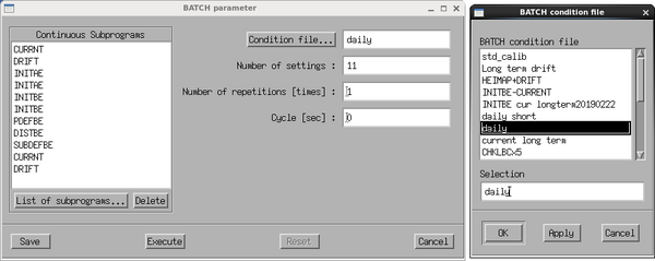
- From the Calibration window choose Commands at the top of the window and click Batch
- From the BATCH parameter window click Condition file...
- Browse for the daily file and click OK
- Click Execute
|
|
Load the daily batch command and execute it. |
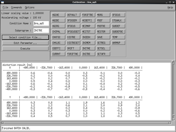
During calibration the system will measure and display the beam position at 49 locations of the writing field. The position error (in nm) can be read of the matrices during execution, an example is shown below. At the end of the process the Calibration window will display Finished BATCH CALIB.
|
|
Example of beam offset matrix shown during auto calibration. Average beam offset is below 1 nm within the 1000 x 1000 µm2 writing field in this example. Image: Thomas Pedersen. |
Measure stage drift
The next step is to measure stage drift. This is done from the Calibration window.
- Select the Drift subprogram and click Execute
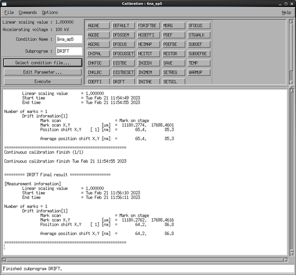
The system will scan the drift mark (BE mark) to determine drift since last drift reset. The absolute value is not important since it is unknown when the drift subprogram was last reset. The time variation of the drift measurements is however important thus one should compare two drift measurements taken 1-2 minutes apart. Luckily the dayli batch command ended with a drift measurement, having made one manually we can now compare the result, see the example below.
|
|
Comparison of two drift measurements. |
In this example the two drift measurements are made a bit more than 1 minute apart (look at timestamps). The x-axis drift has changed from 65.4 nm to 64.2 nm, i.e. a change of 1.2 nm in about 1 minute. The y-axis drift has changed from 85.3 nm to 86.8 nm, a shift of 1.5 nm in about 1 minute. Thus the drift is about 1-1.5 nm/min in this particular example. This is a typical value. If you experience drift of 5-10 nm/min, give the system 10 min to thermally equilibrate and try again. If drift is above 10 nm/min please call the e-beam personnel for assistance.
Measure height profile of sample
The height of the sample surface must be known to focus the electron beam properly at the surface. This can be done using the HEIMAP subprogram.
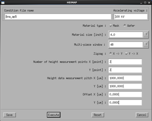
- Select on the HEIMAP subprogram in the Calibration window
- Click Edit Parameter...
- This opens the HEIMAP parameters window, make sure to edit the following parameters
- Check Wafer and not Mask
- Choose correct Material size in the dropdown
- Choose the correct slot ID in Multi-piece window
- Set a reasonable number in x and y Number of height measurement points
- Set a reasonable x- and y-axis pitch in the Height data measurement pitch fields
- Set Offset fields to zero
- Click Save in order to save the setup for execution during exposure
- Click Execute to execute and verify result
|
|
Parameter window of the HEIMAP subprogram. |
The example above will create a 3x3 matrix of height data with a pitch of 1 mm in x and y. After execution the system will display a matrix with height measurement data in µm. Verify that there are no outliers and that variation is less than 100 µm from top to bottom.
Save condition file
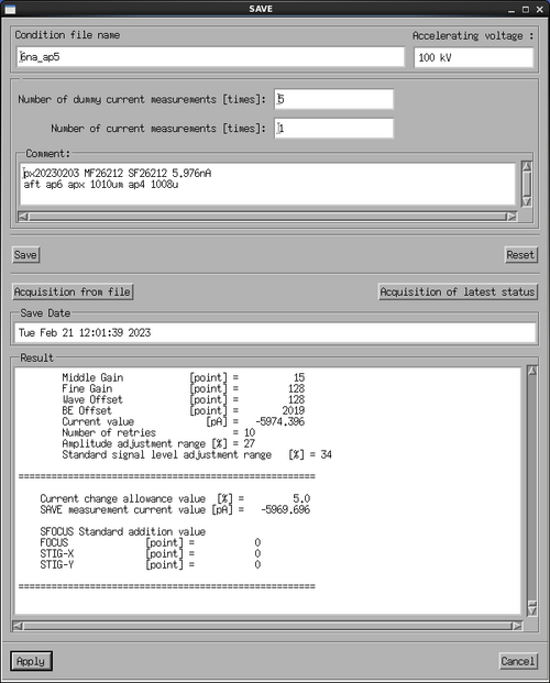
For the calibration data to have effect during exposure the data must be saved into the calibration profile. This is done via the SAVE subprogram from the Calibration window.
- Select the SAVE subprogram
- Click Edit Parameter...
- From the SAVE window click Acquisition of latest status
- Wait 5 seconds for the window to populate with data
- Click Apply and Save
|
|
Acquire the calibration data and then apply the data to save. |
All of the calibration data is now saved and the system is ready for exposure.
Job execution
The job and the system is now ready to execute the exposure.
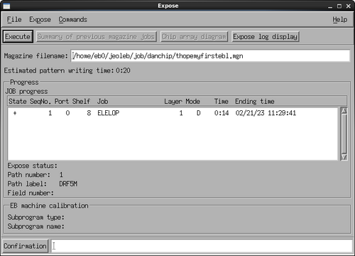
- Open the Expose program from the EBX Menu
- In the Expose program click File and Magazine File...
- Browse for and select the correct file and click OK
- The Expose window is now updated with the file loaded into the Magazine filename: field
- Click Execute
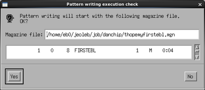
- This opens the Pattern writing execution check window where one can check that the cassette number execution time is as expected before hitting Yes
|
|
Expose window with .mgn file loaded for exposure. Notice that the Progress part of the window still shows the previous exposure information. This field will not update until exposure is started. |
|
|
Use the Pattern writing execution check window to verify the cassette number and estimated execution time. Image: Thomas Pedersen. |
The system will now carry out initial and cyclic calibration as defined by the path in the JDF file and then exposure will start. The pattern writing can be observed in the SSP window (top left) once it starts. Progress can be monitored in the Expose window which will give a completion percentage and completion time for the current sequence. Once exposure is completed the system will confirm this with the Pattern writing completed window.
Table of important subprograms
Below is a brief explanation of some of the most important subprograms found in the Calibration window. The subprograms listed in the blue part of the table are a part of the 'daily' batch of programs.
| Calibration of condition files | |
|---|---|
| Subprogram | Explanation |
| CURRNT | The stage moves the Faraday's cup to the beam and the machine reads the value of the cup. The machine measures the beam current 5 times and calculate the average of the beam current based on these 5 measurements. |
| INITAE | The AE marks (Absorbed Electrons) is a mark type that is connected to a pn-junction, i.e. the current abosrbed in the mark is measured. The AE mark is a knife-edge mark, i.e. is has (originally) very sharp edges. When the beam (with a well-known frequency) scans over this type of mark and absorbed current simultanously is measured, an estimate of the beam diameter can be found. INITAE is a subprogram that finds the AE mark and scans it for testing that the machine can find the mark. |
| INITBE | The BE mark (Backscattered Electrons) is a mark type that consists of a suspended grid of metal. The openings in the grid is 500 microns in both X and Y. When the beam scans over this type of mark, backscattered electrons are detected with the BE detector inside the chamber. This type of mark is used to correlate stage position and beam position during calibration. INITBE is a subprogram that find the BE mark and scans it for testing that the machine can find the mark. |
| SFOCUS | This subprogram finds the minimum beam diameter by scanning an AE mark while changing the focus of the objective lens. The objective lens is defined to be in focus where the machine finds the minimum beam diameter. This program can also be used to observe the depth of focus of a certain condition file. The SFOCUS subprogram does not work well for currents above 6 nA, why SFOCUS is deleted in 'daily' routines of condition files with currents larger than 6 nA. |
| PDEFBE | Using a BE mark, this subprogram corrects deflection gain and rotation of the main deflector. The system positions the BE mark in the corners of the main field (which is a 1000 x 1000 µm2 square) and scans the mark using the primary deflector only. |
| DISTMEM | This subprogram measures the distortion of the beam deflection 7 x 7 positions within the main writing field and generates a distortion correction table. The system positions the BE mark in all 49 positions and uses only the primary deflector to scan the BE mark in every 49 positions. The program sets the distortion directly below the beam (center of the field) to zero. The distortion correction memory in every position in the main writing field is generated by a linear approximation based on the 7 x 7 table. For 0.2 nA or 2 nA, a reasonable convergence value is e.g. 6 nm. |
| DISTBE | This subprogram measures the distortion of the beam deflection 7 x 7 positions within the main writing field and generates a distortion correction table. The system positions the BE mark in all 49 positions and uses only the primary deflector to scan the BE mark in every 49 positions. The program sets the distortion directly below the beam (center of the field) to zero. The distortion correction memory in every position in the main writing field is generated by a cubic approximation based on the 7 x 7 table. For 0.2 nA or 2 nA, a reasonable convergence value is e.g. 8 nm. |
| SUBDEFBE | Using a BE mark, this subprogram corrects deflection gain and rotation of the secondary (sub) deflector. The system positions the BE mark in the corners of the subfield (which is a 4 x 4 µm2 square) and scans the mark using the sub deflector only. |
| DRIFT | This subprograms scans the DRIFT mark. The DRIFT mark can either be a BE mark or an alignment mark on the substrate. By scanning the DRIFT mark during exposure, the machine can positionally adjust the exposed pattern during writing, i.e. positional drift due to cassette heat-up or warm-up during writing can be corrected. This is done by using the the path DRF5M in the jdf-file. |
| HEIMAP | This subprogram measures the height of the substrate to be exposed. The size and workpiece position of the substrate (e.g. 4B) should be entered along with information of desired area to measure height. This area should always be larger than the area of the exposed pattern. The system will focus the beam to the average of the height mesaured in HEIMAP, but only if you expose in mask writing mode (i.e. no aligning) and execute HEIMAP in your initial calibration (e.g. by using path DRF5M). |
| SETWFR | This subprograms scans the global marks of the substrate. You need to enter the theoretical positions of the global marks (in wafer coordinate system) and the offset found during pre-aligning. When SETWFR has succeeded in finding your global marks, it will give you a corrected offset, that should be entered in your sdf-file. |
| CHIPAL | This subprogram scan a set of chip marks on the substrate. You need to enter theoretical position of a chip on your wafer (in wafer coordinate systems) and the theoretical positions of the chip marks on that chip (in chip coordinate system). CHIPAL will then scan 1 or 4 chip marks (mode 1 or mode 4). |
Job execution with alignment
Execution of jobs that require alignment requires a few additional steps compared to the process described above. The additional steps are:
- Optical prealignment of the mounted substrate to determine PQ mark offsets and substrate rotation
- Gain correction to ensure the backscatter detector provides sufficient signal for mark detection using AGCRG
- Verification of PQ mark detection using SETWFR
- Verification of chip mark detection using CHIPAL if chip marks are used
