Specific Process Knowledge/Etch/Etching of Silicon Oxide/SiO2 etch using AOE/Standard recipe with resist mask/AOE SiO2 etch load dependency: Difference between revisions
No edit summary |
|||
| (4 intermediate revisions by the same user not shown) | |||
| Line 1: | Line 1: | ||
'''Feedback to this page''': '''[mailto:labadviser@nanolab.dtu.dk?Subject=Feed%20back%20from%20page%20http://labadviser.nanolab.dtu.dk/index.php/Specific_Process_Knowledge/Etch/Etching_of_Silicon_Oxide/SiO2_etch_using_AOE/Standard_recipe_with_resist_mask/AOE_SiO2_etch_load_dependency click here]''' | '''Feedback to this page''': '''[mailto:labadviser@nanolab.dtu.dk?Subject=Feed%20back%20from%20page%20http://labadviser.nanolab.dtu.dk/index.php/Specific_Process_Knowledge/Etch/Etching_of_Silicon_Oxide/SiO2_etch_using_AOE/Standard_recipe_with_resist_mask/AOE_SiO2_etch_load_dependency click here]''' | ||
{{CC-bghe1}} | |||
=The etch rate dependency of the etch load= | =The etch rate dependency of the etch load= | ||
===Etch load=== | ===Etch load=== | ||
| Line 74: | Line 76: | ||
|- | |- | ||
|} | |} | ||
<br> | |||
[[Image:AOE_SiO2_mresist_etch_rate_vs_etch_load.jpg|left| | [[Image:AOE_SiO2_mresist_etch_rate_vs_etch_load.jpg|left|500px|thumb|By Berit Herstrøm @ DTU Nanolab]] | ||
<br clear="all"/> | |||
===Conclusion=== | ===Conclusion=== | ||
*The etch rate decreases with etch load with aproximately 20% | *The etch rate decreases with etch load with aproximately 20% | ||
*The wafer non-uniformity increases with etch load going from less than ±1% to about ±3% | *The wafer non-uniformity increases with etch load going from less than ±1% to about ±3% | ||
*The selectivity to resist decreases with etch load from about 1:3 to about 1:2 | *The selectivity to resist decreases with etch load from about 1:3 to about 1:2 | ||
Latest revision as of 17:47, 1 February 2023
Feedback to this page: click here
This page is written by Berit Herstrøm @ DTU Nanolab (BGHE) if nothing else is stated
The etch rate dependency of the etch load
Etch load
Etch load is the percentage of the wafer surface that is exposed to the plasma. E.g. if you have a wafer with a surface of SiO2 where 95% of the surface is covered by photoresist (or another masking material that has a high selectivity to SiO2 with the used etcing recipe)the the etch load i 5%
Etch load effect of SiO2 etch with etch recipe SiO2_res and with photoresist as masking material
This work has been done by bghe@nanolab in February/Marts 2013
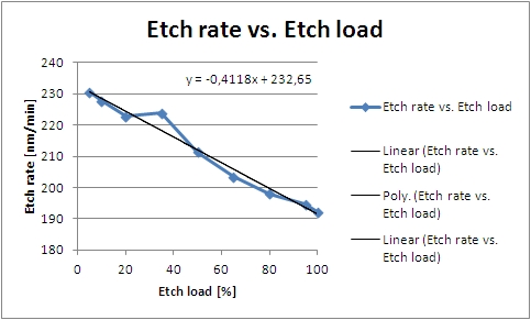
8 wafers with different etch load has been etched with the same recipe in the AOE: m_res_ny (now called SiO2_res 2019-06-26) for the same time and under that same conditions. This was done to isolate the etch load as a parameter to see how much that affects etch rate.
Samples
- 100mm SSP Si wafers 525µm in thickness
- 2.2 µm SiO2 grown in furnace: phospher drive-in, recipe Wet1100 for 10 hours
- 1.4 µm photoresist
- 5%-95% etch load - masks TRAVKA: 5%,10%,20%,35%,50%,65%,80% and 95%
AOE settings
Before each sample etch a 3 min TDESC clean was done to get the chamber in the same condition.
| Parameter | SiO2_res |
|---|---|
| Coil Power | 1300W |
| Platen Power | 200W |
| Platen temperature | 0oC |
| He flow | 174sccm |
| C4F8 flow | 5sccm |
| H2 flow | 4sccm |
| Pressure | 4mTorr |
| Etch time | 4min |
Results
| Ecth load: | 5% | 10% | 20% | 35% | 50% | 65% | 80% | 95% | Comment |
|---|---|---|---|---|---|---|---|---|---|
| Etch rate | 231±1.7nm/min | 228±1.5nm/min | 223±2.3nm/min | 224±2.7nm/min | 211±3.8nm/min | 203±4.6nm/min | 198±5.8nm/min | 192±5.1nm/min | "±" represents the non-uniformity over the wafer |
| Selectivity to resist 1: | 2.9 | 2.8 | 2.7 | 2.5 | 2.4 | 2.3 | 2.0 | 2.0 | |
| Non-uniformity over a 100mm wafer - 1cm exclusion zone | ±0.7% | ±0.7% | ±1.0% | ±1.2% | ±1.8% | ±2.3% | ±2.9% | ±2.7% |
Conclusion
- The etch rate decreases with etch load with aproximately 20%
- The wafer non-uniformity increases with etch load going from less than ±1% to about ±3%
- The selectivity to resist decreases with etch load from about 1:3 to about 1:2
