Specific Process Knowledge/Etch/DRIE-Pegasus/Pegasus-2/ORE with Al2O3 mask: Difference between revisions
No edit summary |
|||
| (162 intermediate revisions by the same user not shown) | |||
| Line 2: | Line 2: | ||
''By Maria Farinha @Nanolab Internal, Jan 2023 if nothing more is stated'' | |||
<!-- | =Al<sub>2</sub>O<sub>3</sub> mask= | ||
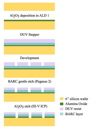
[[File:esq met Al2O3 compact.jpg|400px|right|thumb|'''''Scheme of the sample fabrication using Al<sub>2</sub>O<sub>3</sub> mask. These samples were coated with either 50 or 100 nm of Al<sub>2</sub>O<sub>3</sub>, followed by 65 nm of BARC and 750 nm of DUV resist. Not at scale. <br> | |||
Scheme: Maria Farinha, @DTU Nanolab''''']] | |||
In these samples, the hard mask, Al<sub>2</sub>O<sub>3</sub>, was coated in 150 mm Si wafers using the ALD 1 tool. These sets of samples also had the lithography process done in the DUV stepper to deposit 65 nm of BARC and 750 nm of DUV resist. Three different patterns were created after the development: | |||
# 1 µm width pillars with 1 µm pitch (50 nm Al<sub>2</sub>O<sub>3</sub> + 65 nm BARC + 750 nm DUV resist). | |||
# 1 µm width holes with 1 µm pitch (50 nm Al<sub>2</sub>O<sub>3</sub> + 65 nm BARC + 750 nm DUV resist). | |||
# 200 nm width nanoholes with 400 nm pitch (100 nm Al<sub>2</sub>O<sub>3</sub> + 65 nm BARC + 750 nm DUV resist). | |||
The Si / Al<sub>2</sub>O<sub>3</sub> / BARC / DUV stack was first processed in Pegasus 2 to etch the BARC layer (recipe named ''"barc gentle etch"'', ER=5.42nm/min), and the alumina was etched in the III-V ICP, using a BCl<sub>3</sub> / Ar recipe, which has an ER = 0.45 nm/min. With the pillars and holes samples, the BARC was also etched for 12 min on Pegasus 2, followed by 90 minutes on the III-V ICP. <br> | |||
For the nanoholes, the Al<sub>2</sub>O<sub>3</sub> layer was etched for 260 minutes on the III-V ICP. The next thing would be to etch the BARC layer on Pegasus 2, however, it was seen that after the III-V ICP process, the leftover resist on the sample was removed during the CORE process on Pegasus 2, having no need to do the dedicated ''"barc gentle etch"'' recipe. | |||
<br> | |||
{| border="1" style="text-align: center; width: 800px; height: 200px" | |||
|+ '''Samples profile before going for the ORE process:''' | |||
|- | |||
|-style="background:LightGray; color:Black" | |||
! !! After Al<sub>2</sub>O<sub>3</sub> etch !! Comments | |||
|- | |||
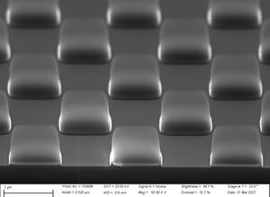
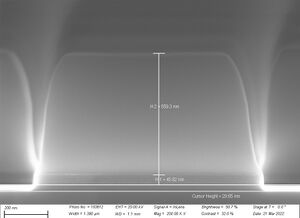
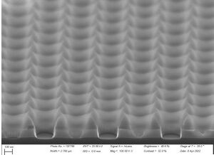
| ''' 1 µm pillars''' || [[File:Pillar 0C+S-RIE Al2O3 02bbbb.jpg|300px]] [[File:Pillar 0C+S-RIE Al2O3 08bbbb.jpg|300px]] || Visible that after the 90 min Al<sub>2</sub>O<sub>3</sub> etch, the mask was correctly etched away confirmed by reaching the silicon (etched ~30nm of it). | |||
|- | |||
| ''' 1 µm holes''' || [[File:bitmapddddd.jpg|300px]] [[File:holes.tif.jpg|300px]] || Visible that after the 90 min Al<sub>2</sub>O<sub>3</sub> etch, the mask was correctly etched away confirmed by reaching the silicon (etched ~16nm of it). | |||
|- | |||
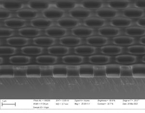
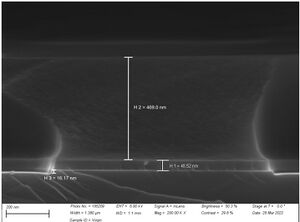
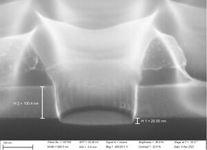
| '''200nm nanoholes''' || [[File:nanoHoles 0g 02 v3.jpg|300px]] [[File:nanoHoles 0g 05 v2.jpg|300px]] || Visible that after the 260 min Al<sub>2</sub>O<sub>3</sub> etch, the mask was correctly etched away confirmed by reaching the silicon (etched ~20nm of it). Resist visible on top of the mask since it was etched during the ORE process. | |||
|} | |||
<br clear="all" /> | |||
=ORE process= | |||
'''''Important!''''' The pressure settings used below '''''may no longer be permitted''''', always check with the Dry etch group. | '''''Important!''''' The pressure settings used below '''''may no longer be permitted''''', always check with the Dry etch group. | ||
| Line 12: | Line 44: | ||
As stated by [https://labadviser.nanolab.dtu.dk/images/5/5c/The_CORE_sequence.pdf '''Nguyen et al.'''], the SF<sub>6</sub> and O<sub>2</sub> fluxes are only separated after 4 s during the C-step. Shorter time steps than that do not execute the function of the clearing. After testing recipes with only 2 s of clearing and with no clear step, it was understood it could be eliminated, showing more depth as well as less undercut when going for shorter cycles. From then on, not CORE but ORE recipes were applied D/E = O/RE. | As stated by [https://labadviser.nanolab.dtu.dk/images/5/5c/The_CORE_sequence.pdf '''Nguyen et al.'''], the SF<sub>6</sub> and O<sub>2</sub> fluxes are only separated after 4 s during the C-step. Shorter time steps than that do not execute the function of the clearing. After testing recipes with only 2 s of clearing and with no clear step, it was understood it could be eliminated, showing more depth as well as less undercut when going for shorter cycles. From then on, not CORE but ORE recipes were applied D/E = O/RE. | ||
<br> | <br> | ||
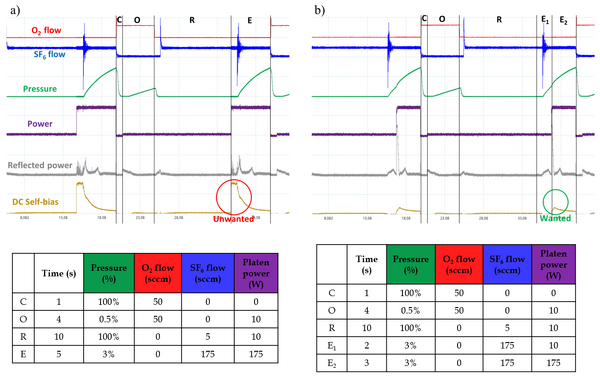
Moreover, during the E-step, the MFC (mass flow controller) presented a delay to read the pressure when compared with the power, creating unwanted bias. To fight it, the E-step was divided into E<sub>1</sub> and E<sub>2</sub>. The E<sub>1</sub> of only 2 s is enough to stabilize the pressure, and E<sub>2</sub> the profile is | Moreover, during the E-step, the MFC (mass flow controller) presented a delay to read the pressure when compared with the power, creating unwanted bias. To fight it, the E-step was divided into E<sub>1</sub> and E<sub>2</sub>. The E<sub>1</sub> of only 2 s is enough to stabilize the pressure, and E<sub>2</sub> the profile is etched correctly, without the unwanted bias. | ||
[[File:graf bias & recipes.png| | [[File:graf bias & recipes.png|600px|center|thumb|'''''CORE process graphics and recipes: a) unwanted DC bias during the E-step; b) E-step separated into two steps, E<sub>1</sub> decreased the bias. <br> | ||
Scheme: Maria Farinha @DTU Nanolab, March 2022''''']] | |||
Going further, the process is set with 4 steps, Oxidize, Removal, E<sub>1</sub> and E<sub>2</sub> steps. In the E<sub>1</sub>, the pressure will rise, without power applied, so for the E<sub>2</sub> the pressure is already rising and the power starts to be applied. | |||
=== Pillars === | === Pillars === | ||
[[File:compare pillars.png| | Using patterned samples of 1 μm pillars with 50 nm of Al<sub>2</sub>O<sub>3</sub>. After the tests, approximately 32nm of Al<sub>2</sub>O<sub>3</sub> were still intact. During the recipe, Pegasus 2 conditions were: Outer EM=10A, T=20°C, no clamping, no He BGC, no coil power and all heaters OFF. | ||
<br clear="all" /> | |||
<br clear="all" /> | |||
[[File:compare pillars.png|400px|left|thumb|'''''Pillars with different etching times. <br> | |||
Photo: Maria Farinha @DTU Nanolab, March 2022''''']] | |||
{| border="1" style="text-align: center; width: 650px; height: 200px" | {| border="1" style="text-align: center; width: 650px; height: 200px" | ||
|+ 1μm Pillar recipe from March 2022 | |+ 1μm Pillar recipe from March 2022 - #244 = 122 min | ||
|-style="background:LightGray; color:Black" | |||
|-style="background: | ! !! Time (s) !! Pressure (valve control) !! O<sub>2</sub> flow (SCCM) !! SF<sub>6</sub> flow (SCCM) !! Platen power (W) | ||
! | |||
|- | |- | ||
| '''O-step''' || 10 || 3% || 200 || 0 || 40 | | '''O-step''' || 10 || 3% || 200 || 0 || 40 | ||
| Line 31: | Line 68: | ||
|- | |- | ||
| '''E<sub>2</sub>-step''' || 7 || 4% || 0 || 350 || 300 | | '''E<sub>2</sub>-step''' || 7 || 4% || 0 || 350 || 300 | ||
|}* Pillars profile effect when varying the etch time. | |||
<br clear="all" /> | |||
=== Holes === | === Holes === | ||
Using patterned samples of 1 μm holes with 50 nm of Al<sub>2</sub>O<sub>3</sub>. After the tests, approximately 28nm of Al<sub>2</sub>O<sub>3</sub> were still intact. When using this recipe, by adjusting the number of cycles, approximately 10 μm was achieved maintaining a straight profile. When going for deeper profiles, 17 μm was also achieved, but the profile started to get positive. Further work may solve the issue. During the recipe, Pegasus 2 conditions were: Outer EM=10A, T=20°C, no clamping, no He BGC and all heaters OFF. | |||
<br clear="all" /> | |||
<br clear="all" /> | |||
[[File:holes 17 e 10 um.png|400px|left|thumb|'''''Holes profile. #144 cycles for 60 min and #288 cycles for 120 min.<br> | |||
Photo: Maria Farinha @DTU Nanolab, March 2022''''']] | |||
{| border="1" style="text-align: center; width: 900px; height: 200px" | |||
|+ '''1μm holes recipe''' | |||
|- | |||
|-style="background:LightGray; color:Black" | |||
! !! Time (s) !! Pressure !! O<sub>2</sub> flow (SCCM) !! SF<sub>6</sub> flow (SCCM) !! Platen power (W) !! Coil power (W) | |||
|- | |||
| '''O-step''' || 10 || 220 mTorr || 200 || 0 || 40 || 0 | |||
|- | |||
| '''R-step''' || 10 || 100% || 0 || 40 || 40 || 0 | |||
|- | |||
| '''E<sub>1</sub>-step''' || 2 || 220 mTorr || 0 || 1200 || 0 || 0 | |||
|- | |||
| '''E<sub>2</sub>-step''' || 1-5 || 220 mTorr || 0 || 1200 || 1 || 2000 | |||
|} * For #288 cycles, 120 min, the profile depth reaches 17.6 μm. For #144 cycles, 60 min, the profile depth reaches 10.1 μm. Width variation presented in the pictures. | |||
<br clear="all" /> | |||
=== Nanoholes === | |||
The nanoholes are 200nm wide, with 400nm pitch with 100 nm Al<sub>2</sub>O<sub>3</sub> mask. During the recipe, Pegasus 2 conditions were: Outer EM=10A, T=20°C, no clamping, no He BGC and all heaters OFF. The removal power was varied, and the achieved ER for 40W was 48.5 nm/min. | |||
<br clear="all" /> | |||
<br clear="all" /> | |||
[[File:nH R-power.png|500px|left|thumb|'''''Nanoholes profile when varying the removal power. <br> | |||
Photo: Maria Farinha @DTU Nanolab, April 2022''''']] | |||
{| border="1" style="text-align: center; width: 650px; height: 200px" | |||
|+ '''200nm nanoholes recipe, varying R-power''' | |||
|- | |||
|-style="background:LightGray; color:Black" | |||
! !! Time (s) !! Pressure (valve control) !! O<sub>2</sub> flow (SCCM) !! SF<sub>6</sub> flow (SCCM) !! Platen power (W) | |||
|- | |||
| '''O-step''' || 10 || 220 mTorr || 200 || 0 || 40 | |||
|- | |||
| '''R-step''' || 10 || 100% || 0 || 40 || * | |||
|- | |||
| '''E<sub>1</sub>-step''' || 2 || 220 mTorr || 0 || 350 || 0 | |||
|- | |||
| '''E<sub>2</sub>-step''' || 0-15 || 220 mTorr || 0 || 350 || 100-300 | |||
|} ''*The R-power value was changed and observed.'' | |||
<br clear="all" /> | |||
The most suitable removal power was 40 W, removing the bottom of the profile correctly without damaging the top part of the profile. | |||
<br clear="all" /> | |||
<br clear="all" /> | |||
[[File:nH E-time.png|500px|left|thumb|'''''Nanoholes profile when varying the ramping E-time .<br> | |||
Photo: Maria Farinha @DTU Nanolab, July 2022''''']] | |||
{| border="1" style="text-align: center; width: 650px; height: 200px" | {| border="1" style="text-align: center; width: 650px; height: 200px" | ||
|+ | |+ '''200nm nanoholes recipe, varying E-ramping time''' | ||
|- | |- | ||
|-style="background: | |-style="background:LightGray; color:Black" | ||
! !! Time (s) !! Pressure (valve control) !! O<sub>2</sub> flow (SCCM) !! SF<sub>6</sub> flow (SCCM) !! Platen power (W) | ! !! Time (s) !! Pressure (valve control) !! O<sub>2</sub> flow (SCCM) !! SF<sub>6</sub> flow (SCCM) !! Platen power (W) | ||
|- | |- | ||
| '''O-step''' || | | '''O-step''' || 10 || 220 mTorr || 200 || 0 || 40 | ||
|- | |- | ||
| '''R-step''' || | | '''R-step''' || 10 || 100% || 0 || 40 || 40 | ||
|- | |- | ||
| '''E<sub>1</sub>-step''' || | | '''E<sub>1</sub>-step''' || 2 || 220 mTorr || 0 || 350 || 0 | ||
|- | |- | ||
| '''E<sub>2</sub>-step''' || | | '''E<sub>2</sub>-step''' || * || 220 mTorr || 0 || 350 || 100-300 | ||
|} | |} ''*The E<sub>2</sub>-time value was changed and observed.'' | ||
<br clear="all" /> | |||
Regarding the measurements of the profiles, in a) the depth reached 3.17 µm with 0-15s of ramping, b) reached 3.21 µm with 1-15s of ramping, c) reached 2.87 µm whit 5-15s of ramping and d) reached 3.63 µm with 15 s without ramping. Even though the etching ramping times may appear similar, there are differences in the feature profile. The ER for 0-15s and 1-15s is around 52 nm/min and for 5-15s and 15s is approximately 48 nm/min. | |||
<br clear="all" /> | |||
=== Isotropic etch === | |||
=== | Some isotropic etches were performed, intercalated with anisotropic etches. The nanoholes are 200nm wide, with 400nm pitch with 100 nm Al<sub>2</sub>O<sub>3</sub> mask. The recipe presented in the table was repeated 2 or 3 times to achieve the picture results. During the recipe, Pegasus 2 conditions were: Outer EM=10A, T=20°C, no clamping, no He BGC and all heaters OFF. Trying to oxide the sample before doing the isotropic etch can help to protect the top part, maintaining a more straight profile. However, after trying to do an oxidation step on Pegasus 2, with 3% valve control. 200 sccm O<sub>2</sub> and 2000W of coil power, the oxide layer was only 3.2 nm. | ||
<br clear="all" /> | |||
<br clear="all" /> | |||
[[File:cpr + iso x2 meas.png|400px|left|thumb|'''''x2 anisotropic + isotropic etch.<br> | |||
Photo: Maria Farinha @DTU Nanolab, June 2022''''']] | |||
{| border="1" | {| border="2" cellpadding="2" cellspacing="1" | ||
| | |+ '''Table: nanoholes + isotropic etch''' | ||
|- | |||
! rowspan="1" align="center"| | |||
| | |||
| Time (s) | |||
| Pressure | |||
| O<sub>2</sub> flow (SCCM) | |||
| SF<sub>6</sub> flow (SCCM) | |||
| Platen power (W) | |||
| Coil power (W) | |||
|- | |||
! rowspan="4" align="center"| Nanoholes etch | |||
| O-step | |||
| 10 | |||
| 220 mTorr | |||
| 200 | |||
| 0 | |||
| 40 | |||
| 0 | |||
|- | |- | ||
|- | | R-step | ||
| 10 | |||
| 100% | |||
| 0 | |||
| 0 | |||
| 40 | |||
| 0 | |||
|- | |- | ||
| | | E<sub>1</sub>-step | ||
| 2 | |||
| 220 mTorr | |||
| 0 | |||
| 350 | |||
| 0 | |||
| 0 | |||
|- | |||
| E<sub>2</sub>-step | |||
| 0-15 | |||
| 220 mTorr | |||
| 0 | |||
| 350 | |||
| 100-300 | |||
| 0 | |||
|- | |- | ||
| | ! rowspan="3" align="center"| Isotropic etch | ||
| O-step | |||
| 30 | |||
| 200 mTorr | |||
| 200 | |||
| 0 | |||
| 0 | |||
| 2000 | |||
|- | |- | ||
| | | R-step | ||
| 30 | |||
| 100% | |||
| 0 | |||
| 40 | |||
| 40 | |||
| 0 | |||
|- | |- | ||
| | | E-step | ||
| 20 | |||
| 200 mTorr | |||
| 0 | |||
| 1200 | |||
| 0 | |||
| 2000 | |||
|- | |||
|} | |} | ||
[[File:cpr + iso x3 meas.png|400px|left|thumb|'''''x3 anisotropic + isotropic etch.<br> | |||
Photo: Maria Farinha @DTU Nanolab, June 2022''''']] | |||
<br clear="all" /> | |||
==Previous work on Peg2== | |||
*[https://run.unl.pt/bitstream/10362/152030/1/Farinha_2022.pdf SF6/O2 Plasma Etching: Optimizing the CORE process and going into 3D Engineering_November22 by Maria Farinha@DTU Nanolab] | |||
Latest revision as of 09:23, 1 May 2023
Feedback to this page: click here
By Maria Farinha @Nanolab Internal, Jan 2023 if nothing more is stated
Al2O3 mask
Scheme: Maria Farinha, @DTU Nanolab
In these samples, the hard mask, Al2O3, was coated in 150 mm Si wafers using the ALD 1 tool. These sets of samples also had the lithography process done in the DUV stepper to deposit 65 nm of BARC and 750 nm of DUV resist. Three different patterns were created after the development:
- 1 µm width pillars with 1 µm pitch (50 nm Al2O3 + 65 nm BARC + 750 nm DUV resist).
- 1 µm width holes with 1 µm pitch (50 nm Al2O3 + 65 nm BARC + 750 nm DUV resist).
- 200 nm width nanoholes with 400 nm pitch (100 nm Al2O3 + 65 nm BARC + 750 nm DUV resist).
The Si / Al2O3 / BARC / DUV stack was first processed in Pegasus 2 to etch the BARC layer (recipe named "barc gentle etch", ER=5.42nm/min), and the alumina was etched in the III-V ICP, using a BCl3 / Ar recipe, which has an ER = 0.45 nm/min. With the pillars and holes samples, the BARC was also etched for 12 min on Pegasus 2, followed by 90 minutes on the III-V ICP.
For the nanoholes, the Al2O3 layer was etched for 260 minutes on the III-V ICP. The next thing would be to etch the BARC layer on Pegasus 2, however, it was seen that after the III-V ICP process, the leftover resist on the sample was removed during the CORE process on Pegasus 2, having no need to do the dedicated "barc gentle etch" recipe.
ORE process
Important! The pressure settings used below may no longer be permitted, always check with the Dry etch group.
As stated by Nguyen et al., the SF6 and O2 fluxes are only separated after 4 s during the C-step. Shorter time steps than that do not execute the function of the clearing. After testing recipes with only 2 s of clearing and with no clear step, it was understood it could be eliminated, showing more depth as well as less undercut when going for shorter cycles. From then on, not CORE but ORE recipes were applied D/E = O/RE.
Moreover, during the E-step, the MFC (mass flow controller) presented a delay to read the pressure when compared with the power, creating unwanted bias. To fight it, the E-step was divided into E1 and E2. The E1 of only 2 s is enough to stabilize the pressure, and E2 the profile is etched correctly, without the unwanted bias.
Scheme: Maria Farinha @DTU Nanolab, March 2022
Going further, the process is set with 4 steps, Oxidize, Removal, E1 and E2 steps. In the E1, the pressure will rise, without power applied, so for the E2 the pressure is already rising and the power starts to be applied.
Pillars
Using patterned samples of 1 μm pillars with 50 nm of Al2O3. After the tests, approximately 32nm of Al2O3 were still intact. During the recipe, Pegasus 2 conditions were: Outer EM=10A, T=20°C, no clamping, no He BGC, no coil power and all heaters OFF.
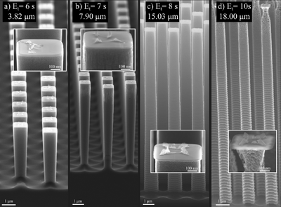
Photo: Maria Farinha @DTU Nanolab, March 2022
| Time (s) | Pressure (valve control) | O2 flow (SCCM) | SF6 flow (SCCM) | Platen power (W) | |
|---|---|---|---|---|---|
| O-step | 10 | 3% | 200 | 0 | 40 |
| R-step | 10 | 100% | 0 | 5 | 40 |
| E1-step | 2 | 4% | 0 | 350 | 40 |
| E2-step | 7 | 4% | 0 | 350 | 300 |
* Pillars profile effect when varying the etch time.
Holes
Using patterned samples of 1 μm holes with 50 nm of Al2O3. After the tests, approximately 28nm of Al2O3 were still intact. When using this recipe, by adjusting the number of cycles, approximately 10 μm was achieved maintaining a straight profile. When going for deeper profiles, 17 μm was also achieved, but the profile started to get positive. Further work may solve the issue. During the recipe, Pegasus 2 conditions were: Outer EM=10A, T=20°C, no clamping, no He BGC and all heaters OFF.

Photo: Maria Farinha @DTU Nanolab, March 2022
| Time (s) | Pressure | O2 flow (SCCM) | SF6 flow (SCCM) | Platen power (W) | Coil power (W) | |
|---|---|---|---|---|---|---|
| O-step | 10 | 220 mTorr | 200 | 0 | 40 | 0 |
| R-step | 10 | 100% | 0 | 40 | 40 | 0 |
| E1-step | 2 | 220 mTorr | 0 | 1200 | 0 | 0 |
| E2-step | 1-5 | 220 mTorr | 0 | 1200 | 1 | 2000 |
* For #288 cycles, 120 min, the profile depth reaches 17.6 μm. For #144 cycles, 60 min, the profile depth reaches 10.1 μm. Width variation presented in the pictures.
Nanoholes
The nanoholes are 200nm wide, with 400nm pitch with 100 nm Al2O3 mask. During the recipe, Pegasus 2 conditions were: Outer EM=10A, T=20°C, no clamping, no He BGC and all heaters OFF. The removal power was varied, and the achieved ER for 40W was 48.5 nm/min.

Photo: Maria Farinha @DTU Nanolab, April 2022
| Time (s) | Pressure (valve control) | O2 flow (SCCM) | SF6 flow (SCCM) | Platen power (W) | |
|---|---|---|---|---|---|
| O-step | 10 | 220 mTorr | 200 | 0 | 40 |
| R-step | 10 | 100% | 0 | 40 | * |
| E1-step | 2 | 220 mTorr | 0 | 350 | 0 |
| E2-step | 0-15 | 220 mTorr | 0 | 350 | 100-300 |
*The R-power value was changed and observed.
The most suitable removal power was 40 W, removing the bottom of the profile correctly without damaging the top part of the profile.

Photo: Maria Farinha @DTU Nanolab, July 2022
| Time (s) | Pressure (valve control) | O2 flow (SCCM) | SF6 flow (SCCM) | Platen power (W) | |
|---|---|---|---|---|---|
| O-step | 10 | 220 mTorr | 200 | 0 | 40 |
| R-step | 10 | 100% | 0 | 40 | 40 |
| E1-step | 2 | 220 mTorr | 0 | 350 | 0 |
| E2-step | * | 220 mTorr | 0 | 350 | 100-300 |
*The E2-time value was changed and observed.
Regarding the measurements of the profiles, in a) the depth reached 3.17 µm with 0-15s of ramping, b) reached 3.21 µm with 1-15s of ramping, c) reached 2.87 µm whit 5-15s of ramping and d) reached 3.63 µm with 15 s without ramping. Even though the etching ramping times may appear similar, there are differences in the feature profile. The ER for 0-15s and 1-15s is around 52 nm/min and for 5-15s and 15s is approximately 48 nm/min.
Isotropic etch
Some isotropic etches were performed, intercalated with anisotropic etches. The nanoholes are 200nm wide, with 400nm pitch with 100 nm Al2O3 mask. The recipe presented in the table was repeated 2 or 3 times to achieve the picture results. During the recipe, Pegasus 2 conditions were: Outer EM=10A, T=20°C, no clamping, no He BGC and all heaters OFF. Trying to oxide the sample before doing the isotropic etch can help to protect the top part, maintaining a more straight profile. However, after trying to do an oxidation step on Pegasus 2, with 3% valve control. 200 sccm O2 and 2000W of coil power, the oxide layer was only 3.2 nm.

Photo: Maria Farinha @DTU Nanolab, June 2022
| Time (s) | Pressure | O2 flow (SCCM) | SF6 flow (SCCM) | Platen power (W) | Coil power (W) | ||
| Nanoholes etch | O-step | 10 | 220 mTorr | 200 | 0 | 40 | 0 |
| R-step | 10 | 100% | 0 | 0 | 40 | 0 | |
| E1-step | 2 | 220 mTorr | 0 | 350 | 0 | 0 | |
| E2-step | 0-15 | 220 mTorr | 0 | 350 | 100-300 | 0 | |
| Isotropic etch | O-step | 30 | 200 mTorr | 200 | 0 | 0 | 2000 |
| R-step | 30 | 100% | 0 | 40 | 40 | 0 | |
| E-step | 20 | 200 mTorr | 0 | 1200 | 0 | 2000 |
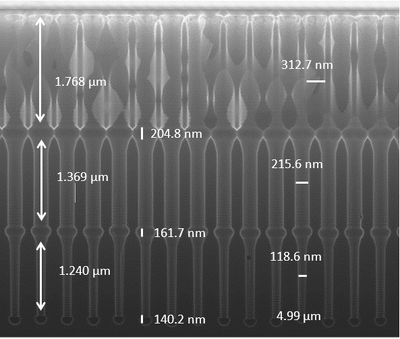
Photo: Maria Farinha @DTU Nanolab, June 2022

