Specific Process Knowledge/Thin film deposition/ALD Picosun R200/HfO2 deposition using ALD new page: Difference between revisions
(Created page with "=HfO<sub>2</sub> standard recipe= ==HfO<sub>2</sub> deposition using TEMAHf and H<sub>2</sub>O precursors== <!-- 20170424A --> The following tables show the recipe and boos...") |
No edit summary |
||
| (131 intermediate revisions by 3 users not shown) | |||
| Line 1: | Line 1: | ||
= | '''Feedback to this page''': '''[mailto:labadviser@nanolab.dtu.dk?Subject=Feed%20back%20from%20page%20http://labadviser.nanolab.dtu.dk/index.php/Specific_Process_Knowledge/Thin_film_deposition/ALD_Picosun_R200/HfO2_deposition_using_ALD_new_page click here]''' | ||
''This page is written by DTU Nanolab internal'' | |||
The | ''The tests have been performed in January-April 2019 by Evgeniy Shkondin, DTU Nanolab.'' | ||
{| border="2" cellspacing="2" cellpadding="5" | |||
The ALD deposition of hafnium oxide (HfO<sub>2</sub>) has been testet in a range between 150 <sup>o</sup>C to 350 <sup>o</sup>C. The precursors used for deposition were tetrakis(ethylmethylamido)hafnium(IV) (TEMAHf) and dionized water. All uniformity results shown on this page have been obtained on new 6" Si(100) wafers with native oxide. XPS, SEM, XRD (not shown) etc. data has been obtained using small test samples. <b>The initial results tested in 2017</b> can be found [[Specific Process Knowledge/Thin film deposition/ALD Picosun R200/HfO2 deposition using ALD|<b>here</b>]]. This page provides updated and additional information on the HfO<sub>2</sub> deposition conditions with modified N<sub>2</sub> flows, precursor boost values and purge times. | |||
=HfO<sub>2</sub> standard recipes= | |||
The <i>TEMAHf</i> precursor is heated to 125 <sup>o</sup>C (TE210) and the heater (TE211 max.) is set to 150 <sup>o</sup>C during deposition. These values may not be exceeded to prevent precursor decomposition. Due to the heating of the precursor the <b>stabilization time needs to be set to 60-180 min</b> in case if precursor needs to be warmed up from room temperature. If it is the second deposition, the stabilization time can be sat to 20 min. Else, there is a probability that an alarm (TE210 PID limit exceeded while pulsing) will be triggered and the process will be stopped after the first pulsing attempt. | |||
<!--%%%%%%%%%%%%%%%%%%%%%%%%%%%%%%%%%%%%%%%%%%%%%%%%%%%%%%%%%%%%%%%%% 150 C %%%%%%%%%%%%%%%%%%%%%%%%%%%%%%%%%%%%%%%%%%%%%%%%%%%%%%%%%%%%%%%%%%%%%%%%%--> | |||
{| border="2" cellspacing="2" cellpadding="2" colspan="3" | |||
|bgcolor="#98FB98" |'''Recipe for deposition of HfO<sub>2</sub> at 150 <sup>o</sup>C ''' | |||
|- | |||
| | |||
{| {{table}} | |||
|align="center" valign="top"| | |||
{|border="2" cellspacing="2" cellpadding="2" align="none" style="width:400px;" | |||
!colspan="3"|Main recipe at 150 <sup>o</sup>C | |||
|- | |||
!<!--blabla--> | |||
|<b> TEMAHf </b> | |||
|<b> H<sub>2</sub>O </b> | |||
|- | |||
! N<sub>2</sub> flow (sccm) | |||
|200 | |||
|100 | |||
|- | |||
! Pulse time (s) | |||
|1.6 | |||
|0.1 | |||
|- | |||
! Purge time (s) | |||
|15 | |||
|10 | |||
|- | |||
|} | |||
|align="center" valign="top"| | |||
{|border="2" cellspacing="2" cellpadding="2" align="none" style="width:400px;" | |||
!colspan="2"|Boost parameters. TEMAHf (master), H<sub>2</sub>O (slave) | |||
|- | |||
!Boost flow (sccm) | |||
|700 | |||
|- | |||
!Pre empty (s) | |||
|0.5 | |||
|- | |||
! Master fill (s) | |||
|1.2 | |||
|- | |||
! Post empty (s) | |||
|0 | |||
|- | |||
|} | |||
|align="center" valign="top"| | |||
{|border="2" cellspacing="2" cellpadding="2" align="none" style="width:400px;" | |||
!colspan="2"|Lines N<sub>2</sub> flow (sccm) | |||
|- | |||
!Line 1 | |||
|100 | |||
|- | |||
!Line 2 | |||
|200 | |||
|- | |||
!Line 3 | |||
|100 | |||
|- | |||
!Line 4 | |||
|40 | |||
|- | |||
|} | |||
|- | |||
|} | |||
|- | |- | ||
|} | |||
<!--%%%%%%%%%%%%%%%%%%%%%%%%%%%%%%%%%%%%%%%%%%%%%%%%%%%%%%%%%%%%%%%%% 200 C %%%%%%%%%%%%%%%%%%%%%%%%%%%%%%%%%%%%%%%%%%%%%%%%%%%%%%%%%%%%%%%%%%%%%%%%%--> | |||
{| border="2" cellspacing="2" cellpadding="2" colspan="3" | |||
|bgcolor="#98FB98" |'''Recipe for deposition of HfO<sub>2</sub> at 200 <sup>o</sup>C ''' | |||
|- | |||
| | | | ||
{| {{table}} | |||
! | |align="center" valign="top"| | ||
{|border="2" cellspacing="2" cellpadding="2" align="none" style="width:400px;" | |||
!colspan="3"|Main recipe at 200 <sup>o</sup>C | |||
|- | |- | ||
! | !<!--blabla--> | ||
| | |<b> TEMAHf </b> | ||
|120 | |<b> H<sub>2</sub>O </b> | ||
|- | |||
! N<sub>2</sub> flow (sccm) | |||
|200 | |||
|120 | |||
|- | |||
! Pulse time (s) | |||
|1.6 | |||
|0.1 | |||
|- | |||
! Purge time (s) | |||
|10 | |||
|10 | |||
|- | |||
|} | |||
|align="center" valign="top"| | |||
{|border="2" cellspacing="2" cellpadding="2" align="none" style="width:400px;" | |||
!colspan="2"|Boost parameters. TEMAHf (master), H<sub>2</sub>O (slave) | |||
|- | |- | ||
! | !Boost flow (sccm) | ||
| | |700 | ||
|- | |- | ||
! | !Pre empty (s) | ||
| | |0.5 | ||
| | |- | ||
! Master fill (s) | |||
|1.2 | |||
|- | |||
! Post empty (s) | |||
|0 | |||
|- | |||
|} | |||
|align="center" valign="top"| | |||
{|border="2" cellspacing="2" cellpadding="2" align="none" style="width:400px;" | |||
!colspan="2"|Lines N<sub>2</sub> flow (sccm) | |||
|- | |- | ||
!Line 1 | |||
|120 | |||
|- | |||
!Line 2 | |||
|200 | |||
|- | |||
!Line 3 | |||
|120 | |||
|- | |||
!Line 4 | |||
|40 | |||
|- | |||
|} | |||
|- | |||
|} | |||
|- | |||
|} | |} | ||
<!--%%%%%%%%%%%%%%%%%%%%%%%%%%%%%%%%%%%%%%%%%%%%%%%%%%%%%%%%%%%%%%%%% 250 C %%%%%%%%%%%%%%%%%%%%%%%%%%%%%%%%%%%%%%%%%%%%%%%%%%%%%%%%%%%%%%%%%%%%%%%%%--> | |||
{| border="2" cellspacing="2" cellpadding="2" colspan="3" | |||
{| border="2" cellspacing="2" cellpadding=" | |bgcolor="#98FB98" |'''Recipe for deposition of HfO<sub>2</sub> at 250 <sup>o</sup>C - 350 <sup>o</sup>C''' | ||
|- | |||
! | | | ||
| | {| {{table}} | ||
|align="center" valign="top"| | |||
{|border="2" cellspacing="2" cellpadding="2" align="none" style="width:400px;" | |||
!colspan="3"|Main recipe at 250 <sup>o</sup>C - 350 <sup>o</sup>C | |||
|- | |- | ||
! | !<!--blabla--> | ||
|0. | |<b> TEMAHf </b> | ||
|<b> H<sub>2</sub>O </b> | |||
|- | |||
! N<sub>2</sub> flow (sccm) | |||
|200 | |||
|150 | |||
|- | |||
! Pulse time (s) | |||
|1.6 | |||
|0.1 | |||
|- | |||
! Purge time (s) | |||
|10 | |||
|10 | |||
|- | |||
|} | |||
|align="center" valign="top"| | |||
{|border="2" cellspacing="2" cellpadding="2" align="none" style="width:400px;" | |||
!colspan="2"|Boost parameters. TEMAHf (master), H<sub>2</sub>O (slave) | |||
|- | |- | ||
!Master fill | !Boost flow (sccm) | ||
|1.2 s | |700 | ||
|- | |||
!Pre empty (s) | |||
|0.5 | |||
|- | |||
! Master fill (s) | |||
|1.2 | |||
|- | |||
! Post empty (s) | |||
|0 | |||
|- | |- | ||
! | |} | ||
| | |align="center" valign="top"| | ||
{|border="2" cellspacing="2" cellpadding="2" align="none" style="width:400px;" | |||
!colspan="2"|Lines N<sub>2</sub> flow (sccm) | |||
|- | |- | ||
!Line 1 | |||
|150 | |||
|- | |||
!Line 2 | |||
|200 | |||
|- | |||
!Line 3 | |||
|150 | |||
|- | |||
!Line 4 | |||
|80 | |||
|- | |||
|} | |||
|- | |||
|} | |||
|- | |||
|} | |} | ||
<!--%%%%%%%%%%%%%%%%%%%%%%%%%%%%%%%%%%%%%%%%%%%%%%%%%%%%%%%%%%%%%%%%% Done %%%%%%%%%%%%%%%%%%%%%%%%%%%%%%%%%%%%%%%%%%%%%%%%%%%%%%%%%%%%%%%%%%%%%%%%%--> | |||
=HfO<sub>2</sub> Ellipsometry results= | |||
The results in this section (uniformity, thickness, refractive index) has been obtained using [[Specific_Process_Knowledge/Characterization/Optical_characterization#Ellipsometer|Ellipsometer VASE]]. HfO<sub>2</sub> thin film on Si has been fitted using <i>Cauchy</i> dispersion relation <math> n(\lambda)=A+\frac{B}{\lambda^{2}}+\frac{C}{\lambda^{4}} </math> with additional expression to describe an exponential Urbach absorption tail at lower wavelengths. | |||
==HfO<sub>2</sub> deposition rate at different temperatures== | |||
In the graphs below the HfO<sub>2</sub> thickness vs. number of cycles for deposition temperatures between 150 <sup>o</sup>C and 350 <sup>o</sup>C presented. Results have been obtained for <100> 150 mm Si wafers with native oxide, based on ellipsometry study. | |||
<gallery caption="Deposition rates of HfO2 at different temperaturs. ALD window." widths="450px" heights="300px" perrow="3"> | |||
image:HfO2_rate_150C.png| Deposition rate of HfO<sub>2</sub> at 150 <sup>o</sup>C. Substrate: Silicon 6" wafer with native oxide. <br> <math> Thickness (nm) = 0.103910 \cdot N - 1.4290 </math> | |||
image:HfO2_rate_200C.png| Deposition rate of HfO<sub>2</sub> at 200 <sup>o</sup>C. Substrate: Silicon 6" wafer with native oxide. <br> <math> Thickness (nm) = 0.092124 \cdot N - 2.0178 </math> | |||
image:HfO2_rate_250C.png| Deposition rate of HfO<sub>2</sub> at 250 <sup>o</sup>C. Substrate: Silicon 6" wafer with native oxide. <br> <math> Thickness (nm) = 0.085887 \cdot N - 4.4988 </math> | |||
image:HfO2_rate_300C.png| Deposition rate of HfO<sub>2</sub> at 300 <sup>o</sup>C. Substrate: Silicon 6" wafer with native oxide. <br> <math> Thickness (nm) = 0.085829 \cdot N - 9.1542 </math> | |||
image:HfO2_rate_350C.png| Deposition rate of HfO<sub>2</sub> at 350 <sup>o</sup>C. Substrate: Silicon 6" wafer with native oxide. <br> <math> Thickness (nm) = 0.092544 \cdot N - 5.1119 </math> | |||
image:rate as a function of temp.png| Deposition rate of HfO<sub>2</sub> as a function of temperature. Substrate: Silicon 6" wafer with native oxide. | |||
</gallery> | |||
==HfO<sub>2</sub> thickness uniformity results== | |||
In the images below the HfO<sub>2</sub> thickness uniformity for deposition temperatures between 150 <sup>o</sup>C and 350 <sup>o</sup>C presented. Results have been obtained for <100> 150 mm Si wafers with native oxide. In total, 17 points has been used in measurements on each wafer. | |||
<gallery caption="Uniformity of HfO2 thickness across 6'' wafer at different temperatures and number of cycles" widths="450px" heights="300px" perrow="3"> | |||
image:HfO2_150C_400cycles.png| Temperature 150 <sup>o</sup>C Silicon 6" wafer with native oxide. | |||
image:HfO2_150C_700cycles.png| Temperature 150 <sup>o</sup>C Silicon 6" wafer with native oxide. | |||
image:HfO2_150C_1000cycles.png| Temperature 150 <sup>o</sup>C Silicon 6" wafer with native oxide. | |||
image:HfO2_200C_400cycles.png| Temperature 200 <sup>o</sup>C Silicon 6" wafer with native oxide. | |||
image:HfO2_200C_700cycles.png| Temperature 200 <sup>o</sup>C Silicon 6" wafer with native oxide. | |||
image:HfO2_200C_1000cycles.png| Temperature 200 <sup>o</sup>C Silicon 6" wafer with native oxide. | |||
image:HfO2_250C_400cycles.png| Temperature 250 <sup>o</sup>C Silicon 6" wafer with native oxide. | |||
image:HfO2_250C_700cycles.png| Temperature 250 <sup>o</sup>C Silicon 6" wafer with native oxide. | |||
image:HfO2_250C_1000cycles.png| Temperature 250 <sup>o</sup>C Silicon 6" wafer with native oxide. | |||
image:HfO2_300C_400cycles.png| Temperature 300 <sup>o</sup>C Silicon 6" wafer with native oxide. | |||
image:HfO2_300C_700cycles.png| Temperature 300 <sup>o</sup>C Silicon 6" wafer with native oxide. | |||
image:HfO2_300C_1000cycles.png| Temperature 300 <sup>o</sup>C Silicon 6" wafer with native oxide. | |||
image:HfO2_350C_400cycles.png| Temperature 350 <sup>o</sup>C Silicon 6" wafer with native oxide. | |||
image:HfO2_350C_700cycles.png| Temperature 350 <sup>o</sup>C Silicon 6" wafer with native oxide. | |||
image:HfO2_350C_1000cycles.png| Temperature 350 <sup>o</sup>C Silicon 6" wafer with native oxide. | |||
</gallery> | |||
=XPS characterization= | |||
<br clear="all" /> | |||
XPS profiles for HfO<sub>2</sub> has been obtained using [[Specific_Process_Knowledge/Characterization/XPS/K-Alpha|XPS K-Alpha]] equipment. | |||
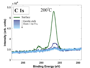
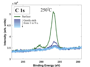
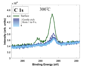
Images below shows the results. The whole XPS spectrum of HfO<sub>2</sub> has been obtained, and the presence of individual elements has been analyzed. The organometallic precursor <i>TEMAHf</i> contains carbon and nitrogen, which makes these elements essential for monitoring and analysis in case of insufficient reaction or precursor decomposition. The analysis of individual elements <i>Hf</i>, <i>O</i>, <i>C</i> and <i>N</i> proceeded with depth profiling. The samples were etched with <i>Ar<sup>+</sup></i> (200eV, low current) from 1 to 9s. with 1s. interval. The gentle etch requires in order to avoid the reduction of HfO<sub>2</sub> due to interaction with the ion beam. It seems that the samples contains a small amount of incorporated carbon (below 2 at. %) which probably comes from Hf precursor. Stoichiometry investigation necessitate more comprehensive analysis of the peak shape. The results revels the ratio of 2.1 to 1 for <i>O</i> to <i>Hf</i> in HfO<sub>2</sub>, this ratio is similar for all temperatures. | |||
<gallery caption="XPS analysis. General measurements and more comprehensive peak fitting. Samples with 400 cycles were selected for all investigations." widths="300px" heights="300px" perrow="4"> | |||
image:HfO2 survey.png| Survey XPS scan of the typical HfO<sub>2</sub> sample. | |||
image:Hf_4f_300C_gentle.png| High resolution <i>Hf 4f</i> scan of the sample prepared at 300 <sup>o</sup>C. Figure shows different depth profiles from surface (green) to 9 s. gentle Ar etch. | |||
image:O_1s_300C_gentle.png| High resolution <i>O 1s</i> scan of the sample prepared at 300 <sup>o</sup>C. Figure shows different depth profiles from surface (green) to 9 s. gentle Ar etch. | |||
image:N_1s_300C_gentle.png| High resolution <i>N 1s</i> scan of the sample prepared at 300 <sup>o</sup>C. Broad peak is probably due to plasmon loss from <i>Hf 4p<sub>3/2</sub></i> in the region. Figure shows different depth profiles from surface (green) to 9 s. gentle Ar etch. | |||
image:C_1s_150C_gentle.png| Investigation of carbon contamination in HfO<sub>2</sub> at 150 <sup>o</sup>C. Initially, the surface is covered with airborn carbon which gives a characteristic high peak (green). Gentle <i>Ar<sup>+</sup></i> sputtering require to clean the surface. A small amount of carbon is found at all temperatures. | |||
image:C_1s_200C_gentle.png| Investigation of carbon contamination in HfO<sub>2</sub> at 200 <sup>o</sup>C. | |||
image:C_1s_250C_gentle.png| Investigation of carbon contamination in HfO<sub>2</sub> at 250 <sup>o</sup>C. | |||
image:C_1s_300C_gentle.png| Investigation of carbon contamination in HfO<sub>2</sub> at 300 <sup>o</sup>C. | |||
image:Hf_4f_comprehensive.png| Comprehensive analysis of <i>Hf 4f</i> peak shape. The measured data (circles) were fitted with Lorentz-Gaussian (L/G) functions (magenta). Taken the appropriate background it is possible to deconvolve the peaks responsible for different bondings. | |||
image:O_1s_comprehensive.png| Comprehensive analysis of <i>O 1s</i> peak shape. | |||
image:Hf_reduction.png| It is very important to use the lowest beam energy as the high energy will reduce HfO<sub>2</sub> to other sates. The figure shows the <i>Hf 4f</i> peak profile with depth etch performed at 3000 eV (highest settings) and high current for 30 to 90 s. Clearly, the reduction changes the surface and preventing analysis. | |||
</gallery> | |||
=SEM inspection= | |||
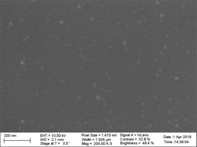
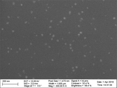
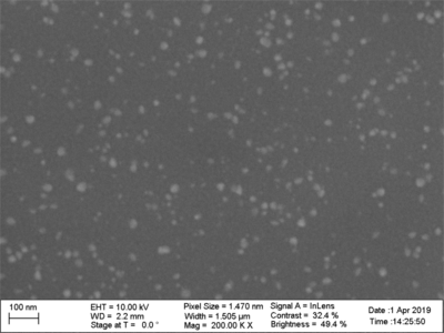
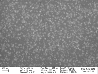
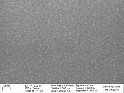
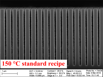
The SEM images of HfO<sub>2</sub> surface morphology for deposition temperatures between 150 <sup>o</sup>C and 350 <sup>o</sup>C. Substrates were pieces of <100> 150 mm Si wafers with native oxide. Magnification is the same on all images (200 kX). The films are mainly amorphous with some degree of polycrystallinity at lowest temperatures. The higher the deposition temperature the more polycrystalline film becomes, and at 350 <sup>o</sup>C the film is mainly composed of polycrystals. The tendency is confirmed by X-ray diffraction analysis (not shown her). | |||
<gallery caption="SEM images of flat surfaces. All films were deposited with 400 cycles." widths="450px" heights="300px" perrow="3"> | |||
image:HfO2_flat_400cycles_150C.png| Flat film of HfO<sub>2</sub> at 150 <sup>o</sup>C. Substrate: Silicon 6" wafer with native oxide. | |||
image:HfO2_flat_400cycles_200C.png| Flat film of HfO<sub>2</sub> at 200 <sup>o</sup>C. Substrate: Silicon 6" wafer with native oxide. | |||
image:HfO2_flat_400cycles_250C.png| Flat film of HfO<sub>2</sub> at 250 <sup>o</sup>C. Substrate: Silicon 6" wafer with native oxide. | |||
image:HfO2_flat_400cycles_300C.png| Flat film of HfO<sub>2</sub> at 300 <sup>o</sup>C. Substrate: Silicon 6" wafer with native oxide. | |||
image:HfO2_flat_400cycles_350C.png| Flat film of HfO<sub>2</sub> at 350 <sup>o</sup>C. Substrate: Silicon 6" wafer with native oxide. | |||
</gallery> | |||
=Deposition of HfO<sub>2</sub> on high aspect ratio structures. Advantages and limitations.= | |||
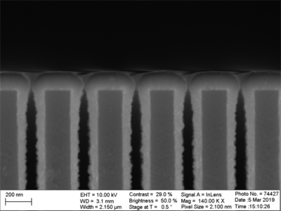
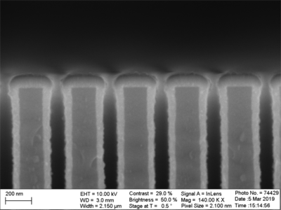
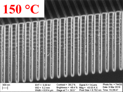
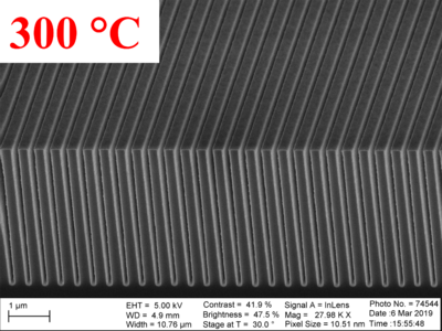
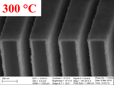
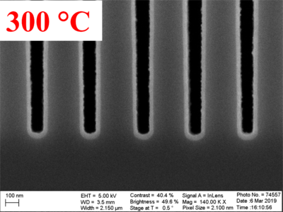
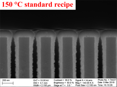
In the figures and images below, the 400 cycles of HfO<sub>2</sub> with temperatures between 150 <sup>o</sup>C and 350 <sup>o</sup>C deposited on Si high aspect ratio trenches presented. The samples were fabricated using [[Specific_Process_Knowledge/Lithography/DUVStepperLithography|DUV Stepper Lithography]] and [[Specific_Process_Knowledge/Etch/DRIE-Pegasus| deep reactive ion etching]]. Trenches are 3µm deep with the period of 400 nm. The standard recipes (presented above) for HfO<sub>2</sub> has been tested for deposition. | |||
==General results== | |||
<gallery caption="Deposition of 400 cycles of HfO2 at different temperatures on high aspect ratio Si trenches." widths="450px" heights="300px" perrow="3"> | |||
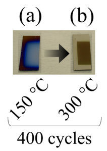
image:image11.png| Photography of all prepared HfO<sub>2</sub> samples at 150<sup>o</sup>C to 350<sup>o</sup>C. Using standart recipes, the uniformity will not be perfect at the 150<sup>o</sup>C and 200<sup>o</sup>C. | |||
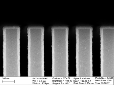
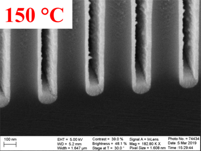
image:t150_full.png| Cross-section SEM image of Si trench with deposited HfO<sub>2</sub> at 150 <sup>o</sup>C. | |||
image:t200_full.png| Cross-section SEM image of Si trench with deposited HfO<sub>2</sub> at 200 <sup>o</sup>C. | |||
image:t250_full.png| Cross-section SEM image of Si trench with deposited HfO<sub>2</sub> at 250 <sup>o</sup>C. | |||
image:t300_full.png| Cross-section SEM image of Si trench with deposited HfO<sub>2</sub> at 300 <sup>o</sup>C. | |||
image:t350_full.png| Cross-section SEM image of Si trench with deposited HfO<sub>2</sub> at 350 <sup>o</sup>C. | |||
</gallery> | |||
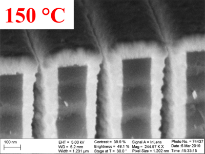
<gallery caption="Deposition of 400 cycles of HfO2 at different temperatures on high aspect ratio Si trenches. In the figures and images below there are SEM images with higher magnification (140kX) which only shows the top part of the trench cross-section." widths="450px" heights="300px" perrow="3"> | |||
image:image11.png| Photography of all prepared HfO<sub>2</sub> samples at 150<sup>o</sup>C to 350<sup>o</sup>C. Using standart recipes, the uniformity will not be perfect at the 150<sup>o</sup>C and 200<sup>o</sup>C. | |||
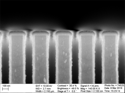
image:t150_top.png| High magnification (140 kX) cross-section SEM image of Si trench with deposited HfO<sub>2</sub> at 150 <sup>o</sup>C. Clearly inhomogeneous deposition, as the thickness on top is sufficiently higher than on the sidewalls. | |||
image:t200_top.png| High magnification (140 kX) cross-section SEM image of Si trench with deposited HfO<sub>2</sub> at 200 <sup>o</sup>C. Inhomogeneous deposition. | |||
image:t250_top.png| High magnification (140 kX) cross-section SEM image of Si trench with deposited HfO<sub>2</sub> at 250 <sup>o</sup>C. Some degree of inhomogeneous deposition. | |||
image:t300_top.png| High magnification (140 kX) cross-section SEM image of Si trench with deposited HfO<sub>2</sub> at 300 <sup>o</sup>C. Conformal deposition. | |||
image:t350_top.png| High magnification (140 kX) cross-section SEM image of Si trench with deposited HfO<sub>2</sub> at 350 <sup>o</sup>C. Conformal deposition. | |||
</gallery> | |||
==Uniformity improvement== | |||
There are two ways to improve the thickness uniformity around the trench structures. The obvious one (and the easiest) is to increase the temperature. Nevertheless, for some users the high temperature is undesirable in case of deposition on temperature sensitive structures or substrates. Also the crystallinity can be a factor, if the user would like to deposit film as amorph as possible it has to be done at low temperature. In this case the recipe can be improved by increasing the purge time between the <i>TEMAHf</i> and water pulses. The disadvantage is the tremendous increase of deposition time. Both approaches can be applied simultaneously for best performance. | |||
<gallery caption="Uniformity improvement." widths="500px" heights="300px" perrow="2"> | |||
image:image33.png| Improvement by increasing of temperature. Deposition of 150<sup>o</sup>C and 300 <sup>o</sup>C for comparison. Standard recipes. | |||
image:image22.png| Improvement by increasing the purge time. It is set to 60 s. after each pulse, making 120 s. in total. | |||
</gallery> | |||
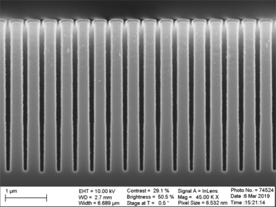
===Increasing temperature=== | |||
SEM images below shows deposition of HfO<sub>2</sub> at temperatures 150<sup>o</sup>C and 300<sup>o</sup>C. Significant improvement of thickness uniformity is achieved at higher temperature. | |||
<gallery caption="SEM images shows the Si trenches with deposited 400 cycles of HfO2 at 150C and 300C." widths="450px" heights="300px" perrow="3"> | |||
image:u1_t150_full.png| Deposition of HfO<sub>2</sub> at 150 <sup>o</sup>C on Si trench. | |||
image:u1_t150_top.png| Deposition of HfO<sub>2</sub> at 150 <sup>o</sup>C on Si trench. | |||
image:u1_t150_buttom.png| Deposition of HfO<sub>2</sub> at 150 <sup>o</sup>C on Si trench. | |||
image:u1_t300_full.png| Deposition of HfO<sub>2</sub> at 300 <sup>o</sup>C on Si trench. | |||
image:u1_t300_top.png| Deposition of HfO<sub>2</sub> at 300 <sup>o</sup>C on Si trench. | |||
image:u1_t300_buttom.png| Deposition of HfO<sub>2</sub> at 300 <sup>o</sup>C on Si trench. | |||
</gallery> | |||
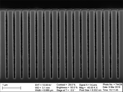
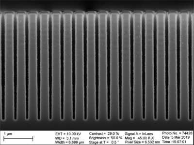
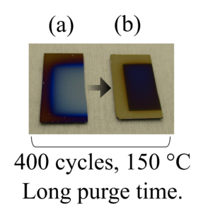
===Increasing purge time=== | |||
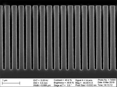
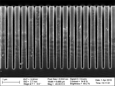
In case there the increase of temperature is not possible, the situation can be improved with the longer purge time. On the SEM images below the uniformity has been improved by changing purge time to 60 s. after each pulse. This means the total time is the number of cycles (400 in this case) has to be multiplied by the total purge time (120 s). The total deposition time is now above 13 hours. The standard deposition of 400 cycles at 150<sup>o</sup>C takes only 2 hours 40 min. | |||
<gallery caption="SEM images shows the Si trenches with deposited 400 cycles of HfO2 at 150C with different purge settings." widths="450px" heights="300px" perrow="2"> | |||
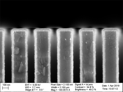
image:u2_t150_full_st.png| Deposition of HfO<sub>2</sub> at 150 <sup>o</sup>C on Si trench. Standard settings. | |||
image:u2_t150_full_lp.png| Deposition of HfO<sub>2</sub> at 150 <sup>o</sup>C on Si trench. Increased purge time to 60+60s. | |||
image:u2_t150_top_st.png| Deposition of HfO<sub>2</sub> at 150 <sup>o</sup>C on Si trench. Standard settings. | |||
image:u2_t150_top_lp.png| Deposition of HfO<sub>2</sub> at 150 <sup>o</sup>C on Si trench. Increased purge time to 60+60s. | |||
</gallery> | |||
Latest revision as of 13:06, 19 June 2023
Feedback to this page: click here
This page is written by DTU Nanolab internal
The tests have been performed in January-April 2019 by Evgeniy Shkondin, DTU Nanolab.
The ALD deposition of hafnium oxide (HfO2) has been testet in a range between 150 oC to 350 oC. The precursors used for deposition were tetrakis(ethylmethylamido)hafnium(IV) (TEMAHf) and dionized water. All uniformity results shown on this page have been obtained on new 6" Si(100) wafers with native oxide. XPS, SEM, XRD (not shown) etc. data has been obtained using small test samples. The initial results tested in 2017 can be found here. This page provides updated and additional information on the HfO2 deposition conditions with modified N2 flows, precursor boost values and purge times.
HfO2 standard recipes
The TEMAHf precursor is heated to 125 oC (TE210) and the heater (TE211 max.) is set to 150 oC during deposition. These values may not be exceeded to prevent precursor decomposition. Due to the heating of the precursor the stabilization time needs to be set to 60-180 min in case if precursor needs to be warmed up from room temperature. If it is the second deposition, the stabilization time can be sat to 20 min. Else, there is a probability that an alarm (TE210 PID limit exceeded while pulsing) will be triggered and the process will be stopped after the first pulsing attempt.
| Recipe for deposition of HfO2 at 150 oC | ||||||||||||||||||||||||||||||||||||||
| ||||||||||||||||||||||||||||||||||||||
| Recipe for deposition of HfO2 at 200 oC | ||||||||||||||||||||||||||||||||||||||
| ||||||||||||||||||||||||||||||||||||||
| Recipe for deposition of HfO2 at 250 oC - 350 oC | ||||||||||||||||||||||||||||||||||||||
| ||||||||||||||||||||||||||||||||||||||
HfO2 Ellipsometry results
The results in this section (uniformity, thickness, refractive index) has been obtained using Ellipsometer VASE. HfO2 thin film on Si has been fitted using Cauchy dispersion relation with additional expression to describe an exponential Urbach absorption tail at lower wavelengths.

HfO2 deposition rate at different temperatures
In the graphs below the HfO2 thickness vs. number of cycles for deposition temperatures between 150 oC and 350 oC presented. Results have been obtained for <100> 150 mm Si wafers with native oxide, based on ellipsometry study.
- Deposition rates of HfO2 at different temperaturs. ALD window.
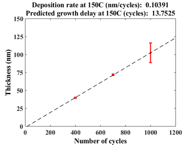
Deposition rate of HfO2 at 150 oC. Substrate: Silicon 6" wafer with native oxide.
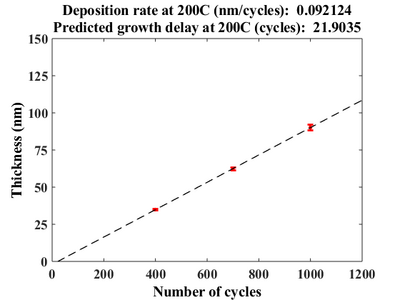
Deposition rate of HfO2 at 200 oC. Substrate: Silicon 6" wafer with native oxide.
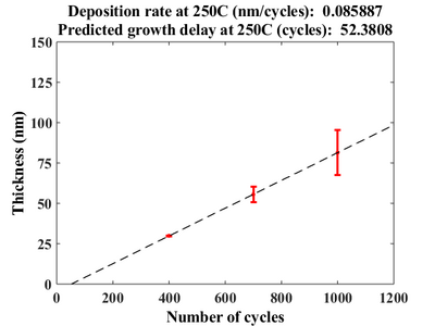
Deposition rate of HfO2 at 250 oC. Substrate: Silicon 6" wafer with native oxide.
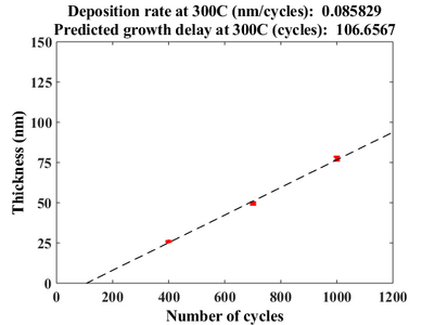
Deposition rate of HfO2 at 300 oC. Substrate: Silicon 6" wafer with native oxide.
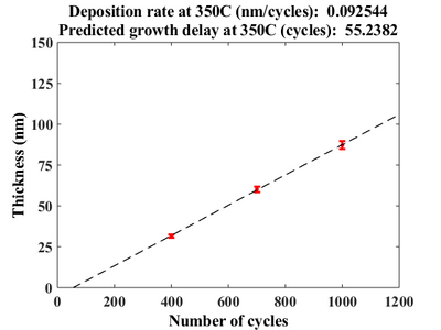
Deposition rate of HfO2 at 350 oC. Substrate: Silicon 6" wafer with native oxide.

Deposition rate of HfO2 as a function of temperature. Substrate: Silicon 6" wafer with native oxide.


HfO2 thickness uniformity results
In the images below the HfO2 thickness uniformity for deposition temperatures between 150 oC and 350 oC presented. Results have been obtained for <100> 150 mm Si wafers with native oxide. In total, 17 points has been used in measurements on each wafer.
- Uniformity of HfO2 thickness across 6 wafer at different temperatures and number of cycles
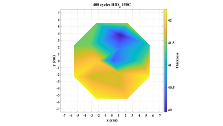
Temperature 150 oC Silicon 6" wafer with native oxide.
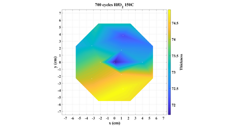
Temperature 150 oC Silicon 6" wafer with native oxide.
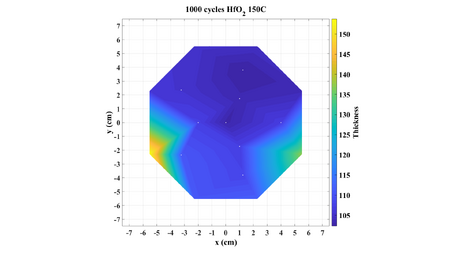
Temperature 150 oC Silicon 6" wafer with native oxide.
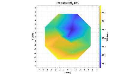
Temperature 200 oC Silicon 6" wafer with native oxide.
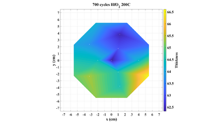
Temperature 200 oC Silicon 6" wafer with native oxide.
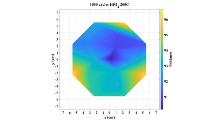
Temperature 200 oC Silicon 6" wafer with native oxide.
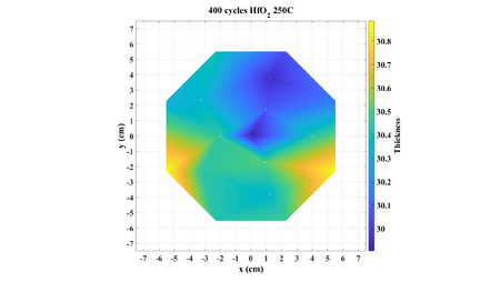
Temperature 250 oC Silicon 6" wafer with native oxide.
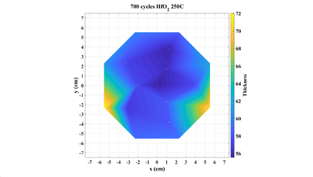
Temperature 250 oC Silicon 6" wafer with native oxide.
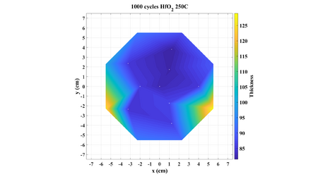
Temperature 250 oC Silicon 6" wafer with native oxide.
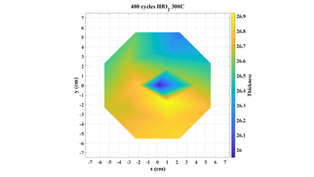
Temperature 300 oC Silicon 6" wafer with native oxide.
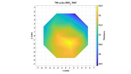
Temperature 300 oC Silicon 6" wafer with native oxide.
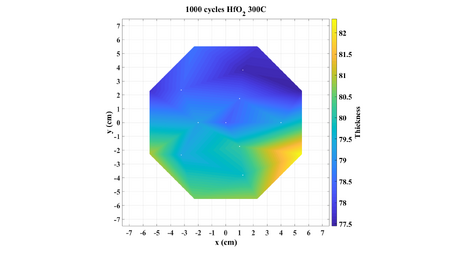
Temperature 300 oC Silicon 6" wafer with native oxide.
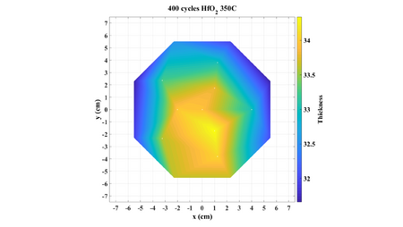
Temperature 350 oC Silicon 6" wafer with native oxide.
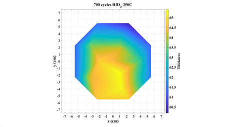
Temperature 350 oC Silicon 6" wafer with native oxide.
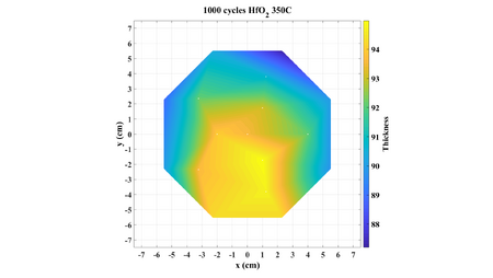
Temperature 350 oC Silicon 6" wafer with native oxide.


XPS characterization
XPS profiles for HfO2 has been obtained using XPS K-Alpha equipment.
Images below shows the results. The whole XPS spectrum of HfO2 has been obtained, and the presence of individual elements has been analyzed. The organometallic precursor TEMAHf contains carbon and nitrogen, which makes these elements essential for monitoring and analysis in case of insufficient reaction or precursor decomposition. The analysis of individual elements Hf, O, C and N proceeded with depth profiling. The samples were etched with Ar+ (200eV, low current) from 1 to 9s. with 1s. interval. The gentle etch requires in order to avoid the reduction of HfO2 due to interaction with the ion beam. It seems that the samples contains a small amount of incorporated carbon (below 2 at. %) which probably comes from Hf precursor. Stoichiometry investigation necessitate more comprehensive analysis of the peak shape. The results revels the ratio of 2.1 to 1 for O to Hf in HfO2, this ratio is similar for all temperatures.
- XPS analysis. General measurements and more comprehensive peak fitting. Samples with 400 cycles were selected for all investigations.
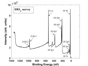
Survey XPS scan of the typical HfO2 sample.
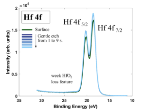
High resolution Hf 4f scan of the sample prepared at 300 oC. Figure shows different depth profiles from surface (green) to 9 s. gentle Ar etch.
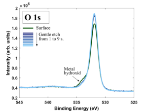
High resolution O 1s scan of the sample prepared at 300 oC. Figure shows different depth profiles from surface (green) to 9 s. gentle Ar etch.
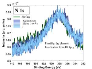
High resolution N 1s scan of the sample prepared at 300 oC. Broad peak is probably due to plasmon loss from Hf 4p3/2 in the region. Figure shows different depth profiles from surface (green) to 9 s. gentle Ar etch.
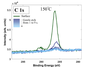
Investigation of carbon contamination in HfO2 at 150 oC. Initially, the surface is covered with airborn carbon which gives a characteristic high peak (green). Gentle Ar+ sputtering require to clean the surface. A small amount of carbon is found at all temperatures.
Investigation of carbon contamination in HfO2 at 200 oC.
Investigation of carbon contamination in HfO2 at 250 oC.
Investigation of carbon contamination in HfO2 at 300 oC.
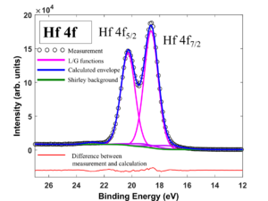
Comprehensive analysis of Hf 4f peak shape. The measured data (circles) were fitted with Lorentz-Gaussian (L/G) functions (magenta). Taken the appropriate background it is possible to deconvolve the peaks responsible for different bondings.
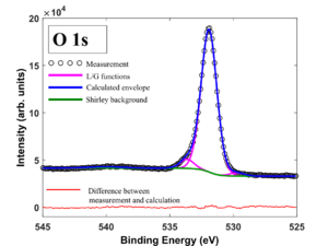
Comprehensive analysis of O 1s peak shape.
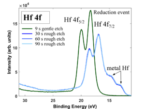
It is very important to use the lowest beam energy as the high energy will reduce HfO2 to other sates. The figure shows the Hf 4f peak profile with depth etch performed at 3000 eV (highest settings) and high current for 30 to 90 s. Clearly, the reduction changes the surface and preventing analysis.


SEM inspection
The SEM images of HfO2 surface morphology for deposition temperatures between 150 oC and 350 oC. Substrates were pieces of <100> 150 mm Si wafers with native oxide. Magnification is the same on all images (200 kX). The films are mainly amorphous with some degree of polycrystallinity at lowest temperatures. The higher the deposition temperature the more polycrystalline film becomes, and at 350 oC the film is mainly composed of polycrystals. The tendency is confirmed by X-ray diffraction analysis (not shown her).
- SEM images of flat surfaces. All films were deposited with 400 cycles.
Flat film of HfO2 at 150 oC. Substrate: Silicon 6" wafer with native oxide.
Flat film of HfO2 at 200 oC. Substrate: Silicon 6" wafer with native oxide.
Flat film of HfO2 at 250 oC. Substrate: Silicon 6" wafer with native oxide.
Flat film of HfO2 at 300 oC. Substrate: Silicon 6" wafer with native oxide.
Flat film of HfO2 at 350 oC. Substrate: Silicon 6" wafer with native oxide.


Deposition of HfO2 on high aspect ratio structures. Advantages and limitations.
In the figures and images below, the 400 cycles of HfO2 with temperatures between 150 oC and 350 oC deposited on Si high aspect ratio trenches presented. The samples were fabricated using DUV Stepper Lithography and deep reactive ion etching. Trenches are 3µm deep with the period of 400 nm. The standard recipes (presented above) for HfO2 has been tested for deposition.
General results
- Deposition of 400 cycles of HfO2 at different temperatures on high aspect ratio Si trenches.
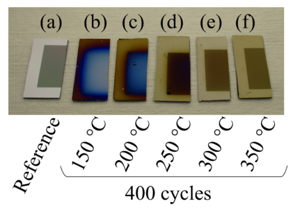
Photography of all prepared HfO2 samples at 150oC to 350oC. Using standart recipes, the uniformity will not be perfect at the 150oC and 200oC.
Cross-section SEM image of Si trench with deposited HfO2 at 150 oC.
Cross-section SEM image of Si trench with deposited HfO2 at 200 oC.
Cross-section SEM image of Si trench with deposited HfO2 at 250 oC.
Cross-section SEM image of Si trench with deposited HfO2 at 300 oC.
Cross-section SEM image of Si trench with deposited HfO2 at 350 oC.


- Deposition of 400 cycles of HfO2 at different temperatures on high aspect ratio Si trenches. In the figures and images below there are SEM images with higher magnification (140kX) which only shows the top part of the trench cross-section.
Photography of all prepared HfO2 samples at 150oC to 350oC. Using standart recipes, the uniformity will not be perfect at the 150oC and 200oC.
High magnification (140 kX) cross-section SEM image of Si trench with deposited HfO2 at 150 oC. Clearly inhomogeneous deposition, as the thickness on top is sufficiently higher than on the sidewalls.
High magnification (140 kX) cross-section SEM image of Si trench with deposited HfO2 at 200 oC. Inhomogeneous deposition.
High magnification (140 kX) cross-section SEM image of Si trench with deposited HfO2 at 250 oC. Some degree of inhomogeneous deposition.
High magnification (140 kX) cross-section SEM image of Si trench with deposited HfO2 at 300 oC. Conformal deposition.
High magnification (140 kX) cross-section SEM image of Si trench with deposited HfO2 at 350 oC. Conformal deposition.


Uniformity improvement
There are two ways to improve the thickness uniformity around the trench structures. The obvious one (and the easiest) is to increase the temperature. Nevertheless, for some users the high temperature is undesirable in case of deposition on temperature sensitive structures or substrates. Also the crystallinity can be a factor, if the user would like to deposit film as amorph as possible it has to be done at low temperature. In this case the recipe can be improved by increasing the purge time between the TEMAHf and water pulses. The disadvantage is the tremendous increase of deposition time. Both approaches can be applied simultaneously for best performance.
- Uniformity improvement.
Improvement by increasing of temperature. Deposition of 150oC and 300 oC for comparison. Standard recipes.
Improvement by increasing the purge time. It is set to 60 s. after each pulse, making 120 s. in total.


Increasing temperature
SEM images below shows deposition of HfO2 at temperatures 150oC and 300oC. Significant improvement of thickness uniformity is achieved at higher temperature.
- SEM images shows the Si trenches with deposited 400 cycles of HfO2 at 150C and 300C.
Deposition of HfO2 at 150 oC on Si trench.
Deposition of HfO2 at 150 oC on Si trench.
Deposition of HfO2 at 150 oC on Si trench.
Deposition of HfO2 at 300 oC on Si trench.
Deposition of HfO2 at 300 oC on Si trench.
Deposition of HfO2 at 300 oC on Si trench.


Increasing purge time
In case there the increase of temperature is not possible, the situation can be improved with the longer purge time. On the SEM images below the uniformity has been improved by changing purge time to 60 s. after each pulse. This means the total time is the number of cycles (400 in this case) has to be multiplied by the total purge time (120 s). The total deposition time is now above 13 hours. The standard deposition of 400 cycles at 150oC takes only 2 hours 40 min.
- SEM images shows the Si trenches with deposited 400 cycles of HfO2 at 150C with different purge settings.
Deposition of HfO2 at 150 oC on Si trench. Standard settings.
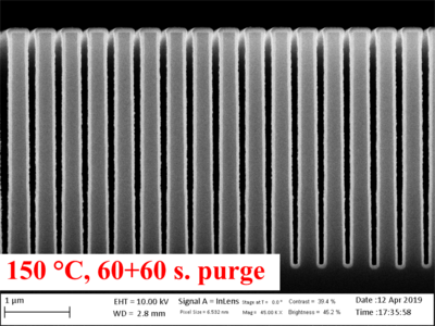
Deposition of HfO2 at 150 oC on Si trench. Increased purge time to 60+60s.
Deposition of HfO2 at 150 oC on Si trench. Standard settings.
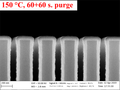
Deposition of HfO2 at 150 oC on Si trench. Increased purge time to 60+60s.


