LabAdviser/Technology Research/Organic Ice Resists for Electron-Beam Lithography - Instrumentation and Processes/Electron-Beam Lithography on Organic Ice Resists: Difference between revisions
| (One intermediate revision by the same user not shown) | |||
| Line 17: | Line 17: | ||
==Organic Ice Resists== | ==Organic Ice Resists== | ||
[[File:Comparison1_OIR.PNG|400px]] | |||
Vapour pressure is the tabulated value at room temperature. Freezing temperature is the tabulated value at atmospheric pressure. | |||
[[File:Comparison2_OIR.PNG|400px]] | |||
Thickness ranges are suggestions based on our experience, and are measured after sublimation via AFM. | |||
==Contrast Curve== | ==Contrast Curve== | ||
[[File:Contrast_OIR.png|600px]] | |||
==Multi-layers== | ==Multi-layers== | ||
Latest revision as of 14:29, 15 June 2018
Feedback to this page: click here
Electron-Beam Lithography on Organic Ice Resists
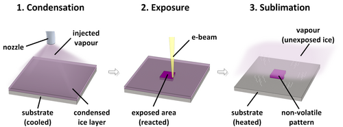
Simple organic molecules, e.g. alcohols, condensed to form thin-films at low temperature demonstrate resist-like capabilities for EBL applications and beyond. The entire lithographic process takes place in a single instrument, and avoids exposing users to chemicals and the need of cleanrooms. Unlike EBL that requires large samples with optically flat surfaces, we patterned on fragile membranes only 5 nm-thin, and 2×2 mm2 diamond samples. We created patterns on the nanometer to sub-millimeter scale, as well as three-dimensional structures by stacking layers of frozen organic molecules. Finally, using plasma etching, the organic ice resist (OIR) patterns are used to structure the underlying material, and thus enable nanodevice fabrication.
Overview
Resist thickness ranged between 7 nm up to 2 µm, with best results obtained for films around 20-200 nm, deposited in 5-10 min.
Critical dose was dependent on acceleration voltage and OIR, with the lowest observed at 3 mC/cm2 for nonane OIR exposed at 5 keV. The resolution achievable with the SEM LEO was limited to above 50 nm due to vibrations in the column and stage; still, an alternative cryo-ETEM setup at DTU Cen was developed from the project confirming sub-10 nm resolution.
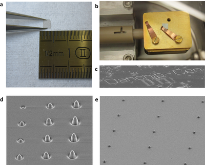
A variety of sample geometries was tested in the SEM tool, as small as 2 mm in size and as thin as 5 nm membranes. Their patterning could be accommodated at no added effort, as with IL.
Organic Ice Resists
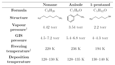
Vapour pressure is the tabulated value at room temperature. Freezing temperature is the tabulated value at atmospheric pressure.
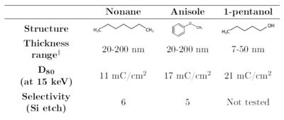
Thickness ranges are suggestions based on our experience, and are measured after sublimation via AFM.
Contrast Curve
Multi-layers
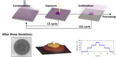
The unique patterning setup (all-in-one) allowed complex in-situ deposition strategies. EBL routines for multi-layer and three-dimensional structuring were demonstrated. This opened up a wide range of possible directions to pursue in the future with this technique.
Etching

As other organic lithographic resists, OIR patterns are able to withstand the chemical and physical action of reactive species protecting the underlying material, while the surrounding areas are gradually removed.
We initially demonstrated this process to create silicon nanostructures on the sample surface. The silicon etch consisted of a two-phase Bosch process iterating an isotropic etching step based on SF6 plasma and a sidewall passivation step. For nonane ice patterns, selectivity over silicon was 1:6, which is the same value obtained with AR-N 7520.
We then used similar samples made from silicon wafers with a layer of silicon oxide thermally grown on its surface. We structured the SiO2 layer using patterned OIR features as mask in one of our cleanroom's oxide RIE tools for photoresist. The recipe consisted in a single step, a continuous flow etch based on C4F8. The oxide etch process resulted in rougher and more shallow lines, due to limited etch resistance. The selectivity for the SiO2 RIE was 1:1.6; the corresponding value for AR-N 7520 was not measured since the profiles were not satisfying, requiring further optimization.
Diamond Nanofabrication
We defined OIR patterns onto diamond chips as small as 2x2 mm2 to be used as etch mask. OIR layers of well-controlled thickness can be deposited on the entire sample surface, regardless of the shape and sharp corners of the diamond chip, and the one-step lithography reduces manipulating these small samples to a minimum.
To obtain a deeper etch, diamond chips were coated with 10 nm ALD Al2O3 to act as a hard mask, and then a OIR was deposited and patterned.
Due to the insulating nature of diamond, localized charging was occasionally observed, resulting in distortion and displacement of the desired layout in denser exposure areas. A thin Al layer was added on top of the sample to ground it through the SEM clip, which solved the issue without affecting the following etch steps.

