Specific Process Knowledge/Characterization/KLA-Tencor Surfscan 6420: Difference between revisions
Jump to navigation
Jump to search
THIS PAGE IS UNDER CONSTRUCTION
| Line 51: | Line 51: | ||
|style="background:LightGrey; color:black"|Batch size | |style="background:LightGrey; color:black"|Batch size | ||
|style="background:WhiteSmoke; color:black"| | |style="background:WhiteSmoke; color:black"| | ||
*Small wafer pieces can all be used | |||
*1-25 100 mm wafers | *1-25 100 mm wafers | ||
*1-25 150 mm wafers | *1-25 150 mm wafers | ||
*1-25 200 mm wafers | |||
|- | |- | ||
| style="background:LightGrey; color:black"|Substrate material allowed | | style="background:LightGrey; color:black"|Substrate material allowed | ||
Revision as of 14:41, 23 April 2013
THIS PAGE IS UNDER CONSTRUCTION
Feedback to this page: click here
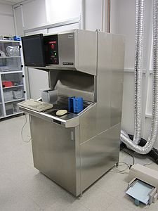
KLA-Tencor Surfscan 6420
Particles counting of a unpatterned surface. A broad range of particles size from 0.1 µm to greater than 3 µm can be measured on a polished silicon or epitaxial layers. Thin films as e.g. Poly-si, Nitride and thermal Oxide can also be inspected. The system will remove small surface roughness so it not count as a particle.
The user manual(s), quality control procedure(s) and results, user APV(s), technical information and contact information can be found in LabManager:
| Purpose |
| |
|---|---|---|
| Performance | Particles size |
|
| Througput |
| |
| Repeatbility |
| |
| Process parameter range | Process Temperature |
|
| Process pressure |
| |
| Substrates | Batch size |
|
| Substrate material allowed |
