Specific Process Knowledge/Etch/RIE (Reactive Ion Etch): Difference between revisions
No edit summary |
|||
| Line 15: | Line 15: | ||
|- | |- | ||
!style="background:silver; color:black;" align="left"|Purpose | !style="background:silver; color:black;" align="left"|Purpose | ||
|style="background:LightGrey; color:black"| | |style="background:LightGrey; color:black"|Dry etch of ||style="background:WhiteSmoke; color:black"| | ||
*Silicon | |||
*Silicon oxide | *Silicon oxide | ||
*Silicon | *Silicon (oxy)nitride | ||
|- | |- | ||
!style="background:silver; color:black" align="left"|Performance | !style="background:silver; color:black" align="left"|Performance | ||
|style="background:LightGrey; color:black"| | |style="background:LightGrey; color:black"|Etch rates||style="background:WhiteSmoke; color:black"| | ||
*~ | *Silicon: ~0.04-0.8 µm/min | ||
*Silicon oxide:~0.02-0.15 µm/min | |||
*Silicon (oxy)nitride:~0.02-? µm/min | |||
|- | |- | ||
|style="background:silver; color:black" |.||style="background:LightGrey; color:black"| | |style="background:silver; color:black" |.||style="background:LightGrey; color:black"|Anisotropy||style="background:WhiteSmoke; color:black"| | ||
*~ | *~Can vary from isotropic to anisotropic with vertical sidewalls and on to a physical etch were the sidewalls are angled but without etching under the mask. | ||
|- | |- | ||
|style="background:silver; color:black"|.||style="background:LightGrey; color:black"|Process pressure | |style="background:silver; color:black"|.||style="background:LightGrey; color:black"|Process pressure | ||
|style="background:WhiteSmoke; color:black"| | |style="background:WhiteSmoke; color:black"| | ||
*~200 | *~20-200 mTorr | ||
|- | |- | ||
|style="background:silver; color:black"|.||style="background:LightGrey; color:black"|Gas flows | |style="background:silver; color:black"|.||style="background:LightGrey; color:black"|Gas flows | ||
|style="background:WhiteSmoke; color:black"| | |style="background:WhiteSmoke; color:black"| | ||
* | *SF<math>_6</math>: sccm | ||
* | *O<math>_2</math>O: sccm | ||
* | *CHF<math>_3</math>: sccm | ||
* | *CF<math>_4</math>: sccm | ||
*H<math>_2</math>: sccm | |||
* | *C<math>_2</math>F<math>_6</math>: sccm | ||
* | |||
|- | |- | ||
!style="background:silver; color:black" align="left"|Substrates | !style="background:silver; color:black" align="left"|Substrates | ||
|style="background:LightGrey; color:black"|Batch size | |style="background:LightGrey; color:black"|Batch size | ||
|style="background:WhiteSmoke; color:black"| | |style="background:WhiteSmoke; color:black"| | ||
*1 | *1 4" wafer per run | ||
*1 | *1 2" wafer per run | ||
*Or several | *Or several smaller pieces | ||
|- | |- | ||
|style="background:silver; color:black"|.|| style="background:LightGrey; color:black"|Substrate material allowed | |style="background:silver; color:black"|.|| style="background:LightGrey; color:black"|Substrate material allowed | ||
| Line 71: | Line 54: | ||
**with layers of silicon oxide or silicon (oxy)nitride | **with layers of silicon oxide or silicon (oxy)nitride | ||
*Quartz wafers | *Quartz wafers | ||
|- | |||
|style="background:silver; color:black"|.|| style="background:LightGrey; color:black"|Possible masking material | |||
|style="background:WhiteSmoke; color:black"| | |||
*Silicon/PolySi | |||
*Silicon oxide or silicon (oxy)nitride | |||
*Aluminium | |||
*Other metals if the coverage is <5% of the wafer area | |||
|- | |- | ||
|style="background:silver; color:black"|.|| style="background:LightGrey; color:black"|Material allowed on the substrate | |style="background:silver; color:black"|.|| style="background:LightGrey; color:black"|Material allowed on the substrate | ||
Revision as of 12:06, 5 December 2007
Etching using the dry etch technique RIE (Reactive Ion Etch)
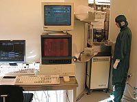
At Danchip we have three RIE's. Two (RIE1 and RIE2) for etching silicon based materials (silicon, silicon oxide, sillicon nitride) and one (III-V RIE) for etching III-V materials (is discussed under III-V processing). The hardware of RIE1 and RIE2 is very similar but you cannot count on that identical recipes on RIE1 and RIE2 perform exactly the same. In addition to that the main difference between RIE1 and RIE2 is the cleanness of the two equipment. In rough terms RIE1 is the clean system and the RIE2 is the dirty system. This means that in RIE2 opposed to RIE1 it is allowed have small amounts of metals exposed to the plasma. Look in the manuals for RIE1 and RIE2 to read the details for this difference (you can find the manuals in LabManager [1]).
Process information
| Purpose | Dry etch of |
|
|---|---|---|
| Performance | Etch rates |
|
| . | Anisotropy |
|
| . | Process pressure |
|
| . | Gas flows |
|
| Substrates | Batch size |
|
| . | Substrate material allowed |
|
| . | Possible masking material |
|
| . | Material allowed on the substrate |
|


