Specific Process Knowledge/Etch/Etching of Silicon/Si etch using RIE1 or RIE2: Difference between revisions
Jump to navigation
Jump to search
| Line 56: | Line 56: | ||
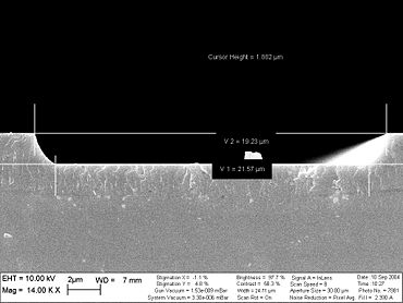
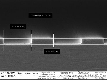
The etching results are dependent on the mask geometry primarily the etch load (meaning the area of the silicon substrate that is exposed to the plasma). To illustrate that you can see on the images below the OH_PolyA recipe tested on two different mask layout. The first one has a load of 10-20% and the second has a load of 50%. | The etching results are dependent on the mask geometry primarily the etch load (meaning the area of the silicon substrate that is exposed to the plasma). To illustrate that you can see on the images below the OH_PolyA recipe tested on two different mask layout. The first one has a load of 10-20% and the second has a load of 50%. | ||
[[image:Rie1_load10_ohpolya.jpg| | [[image:Rie1_load10_ohpolya.jpg|370x370px|thumb|left|RIE1: OH_Polya on load ~10% 4 min.]] | ||
[[image:RIE1-50load_ohpolya.jpg| | [[image:RIE1-50load_ohpolya.jpg|370x370px|thumb|RIE1: OH_Polya on load 50% 4 min.]] | ||
Revision as of 14:06, 9 November 2007
RIE (Reactive Ion Etch) can be used for etching silicon - both crystalline and polycrystalline silicon. The etch can be isotropic or anisotropic with vertical sidewalls depending on the process recipe and the masking material and geometry. The Si is etched by flour radicals that are created from SF6(g) in a RF generated plasma.
The silicon substrate:
Most be a wafer of 4" or below or small pieces, not higher than about 2mm.
The silicon can be masked by these materials:
- Photoresist
- E-beam resist
- Silicon Oxide
- Silicon Nitride
- Aluminium
- Chromium (ONLY RIE2!)
- Other metals if they cover less than 5% of the wafer area (ONLY RIE2!)
Most used recipe (this recipe is being watched in the in the quality assurance program)
| Recipe: | OH_POLYA |
|---|---|
| SF6 flow | 32 sccm |
| O2 flow | 8 sccm |
| Pressure | 80 mTorr |
| RF-power | 30 W |
| Expected results in RIE1 | Expected results in RIE2 | |
|---|---|---|
| Etch rate in Si | ~0.40 µm/min | ~0.45 µm/min |
| Etch rate in Si3N4 | ~0.05 µm/min | |
| Etch rate in SiO2 | ~0.02 µm/min |
The etching results are dependent on the mask geometry primarily the etch load (meaning the area of the silicon substrate that is exposed to the plasma). To illustrate that you can see on the images below the OH_PolyA recipe tested on two different mask layout. The first one has a load of 10-20% and the second has a load of 50%.

