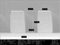
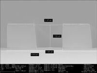
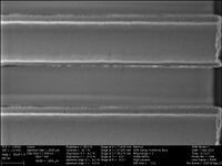
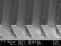
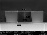
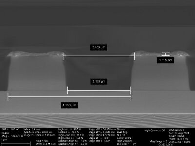
Specific Process Knowledge/Etch/DRIE-Pegasus/Pegasus-4/SiO2 Etch/Cr mask: Difference between revisions
No edit summary |
|||
| (94 intermediate revisions by the same user not shown) | |||
| Line 1: | Line 1: | ||
'''Feedback to this page''': '''[mailto:labadviser@nanolab.dtu.dk?Subject=Feed%20back%20from%20page%20http://labadviser.nanolab.dtu.dk/index.php/Specific_Process_Knowledge/Etch/DRIE-Pegasus/Pegasus-4/SiO2_Etch/Cr_mask click here]'''<br> | '''Feedback to this page''': '''[mailto:labadviser@nanolab.dtu.dk?Subject=Feed%20back%20from%20page%20http://labadviser.nanolab.dtu.dk/index.php/Specific_Process_Knowledge/Etch/DRIE-Pegasus/Pegasus-4/SiO2_Etch/Cr_mask click here]'''<br> | ||
{{CC-bghe2}} | {{CC-bghe2}} | ||
=SiO2 trench etching with Cr mask= | |||
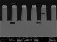
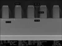
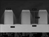
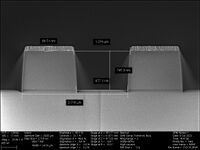
[[test12]] | |||
{| border="2" cellspacing="2" cellpadding="3" | {| border="2" cellspacing="2" cellpadding="3" | ||
| Line 42: | Line 46: | ||
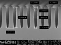
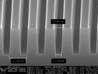
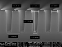
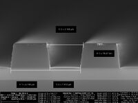
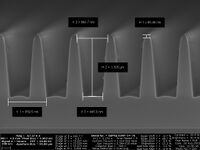
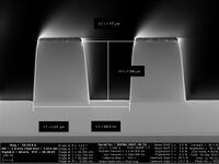
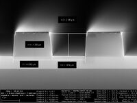
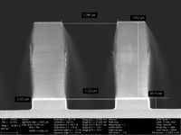
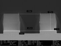
*100 nm Cr mask etched in ICP metal with 500nm DUV neg resist (NUV 2300-0.5) and 65 nm barc. | *100 nm Cr mask etched in ICP metal with 500nm DUV neg resist (NUV 2300-0.5) and 65 nm barc. | ||
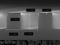
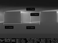
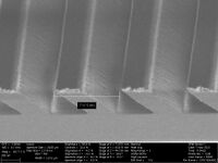
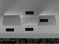
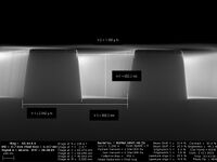
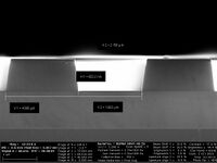
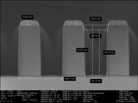
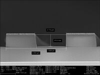
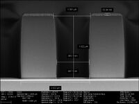
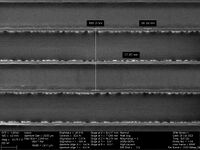
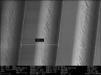
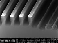
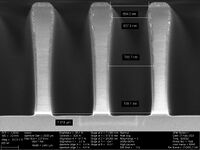
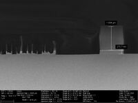
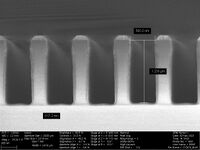
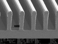
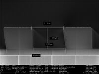
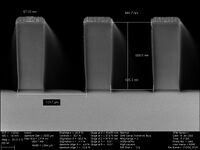
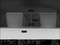
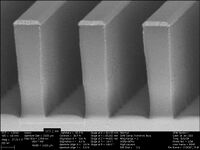
===Results | [[File:C041696Cr_01.jpg|400px|thumb|left|Cr mask before SiO2 etch 800 nm pitch 50% duty cycle. The The Cr linewidth is clearly less than designed]] | ||
<br clear="all" /> | |||
==Results== | |||
{| border="2" cellspacing="2" cellpadding="3" | {| border="2" cellspacing="2" cellpadding="3" | ||
|'''Temporary conclusions on how the process parameters affect the results in this study:''' | |'''Temporary conclusions on how the process parameters affect the results in this study:''' | ||
|'''What process parameters affect the results?''' | |'''What process parameters affect the results?''' | ||
|- | |- style="vertical-align:top;" | ||
| | | | ||
*Going from full wafer to small piece on Si carrier: | *Going from full wafer to small piece on Si carrier: | ||
| Line 79: | Line 86: | ||
|- | |- | ||
|} | |} | ||
===Profile SEM images=== | |||
{| border="2" cellspacing="2" cellpadding="3" style="width: 100%;" | |||
!style="width: 20%"|Recipe settings | |||
!style="width: 10%"|Comments | |||
!style="width: 70%"|SEM gallery | |||
|- style="vertical-align:top;" | |||
| | |||
*'''On 6" wafer''' | |||
*Coil Power [W]:2500 | |||
*Platen Power [W]: 200 | |||
*Platen temperature [<sup>o</sup>C]: 20 | |||
*H2 flow [sccm]:25.6 | |||
*C<sub>4</sub>F<sub>8</sub> flow [sccm]: 25.6 | |||
*He flow [sccm]:448.7 | |||
*Pressure:Fully open APC valve (8-9 mTorr) | |||
*Electromagnetic coils (EM) 'outer coil' / 'inner coil':'2 A' / '30 A' | |||
*PLEASE DO NOT RUN WITH THESE SETTINGS FOR MORE THAN 6 MIN | |||
|text | |||
| | |||
<gallery caption="SiO2 etch with Cr mask on full wafer 6 min etch" perrow="6" widths="200px" heights="150px"> | <gallery caption="SiO2 etch with Cr mask on full wafer 6 min etch" perrow="6" widths="200px" heights="150px"> | ||
| Line 89: | Line 114: | ||
File:C09721_center_22.jpg | File:C09721_center_22.jpg | ||
</gallery> | </gallery> | ||
|- style="vertical-align:top;" | |||
| | |||
*'''Piece on Si carrier''' | |||
*Coil Power [W]:2500 | |||
*Platen Power [W]: 200 | |||
*Platen temperature [<sup>o</sup>C]: 20 | |||
*H2 flow [sccm]:25.6 | |||
*C<sub>4</sub>F<sub>8</sub> flow [sccm]: 25.6 | |||
*He flow [sccm]:448.7 | |||
*Pressure:Fully open APC valve (8-9 mTorr) | |||
*Electromagnetic coils (EM) 'outer coil' / 'inner coil':'2 A' / '30 A' | |||
*PLEASE DO NOT RUN WITH THESE SETTINGS FOR MORE THAN 6 MIN | |||
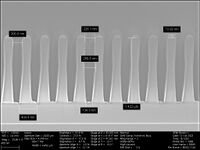
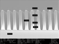
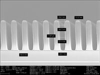
|More sidewall passivation on chip than on full wafer | |||
| | |||
<gallery caption="SiO2 etch with Cr mask on wafer piece on Si carrier 6 min etch" perrow="6" widths="200px" heights="150px"> | <gallery caption="SiO2 etch with Cr mask on wafer piece on Si carrier 6 min etch" perrow="6" widths="200px" heights="150px"> | ||
| Line 99: | Line 137: | ||
File:C10022_03__12.jpg | File:C10022_03__12.jpg | ||
</gallery> | </gallery> | ||
|- style="vertical-align:top;" | |||
| | |||
*Coil Power [W]:2500 | |||
*Platen Power [W]: 200 | |||
*Platen temperature [<sup>o</sup>C]: 20 | |||
*'''H2 flow [sccm]:0''' | |||
*C<sub>4</sub>F<sub>8</sub> flow [sccm]: 25.6 | |||
*He flow [sccm]:448.7 | |||
*Pressure:Fully open APC valve (8-9 mTorr) | |||
*Electromagnetic coils (EM) 'outer coil' / 'inner coil':'2 A' / '30 A' | |||
*PLEASE DO NOT RUN WITH THESE SETTINGS FOR MORE THAN 6 MIN | |||
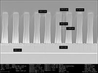
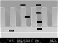
|Less sidewall passivation from removing the H2 | |||
| | |||
<gallery caption="SiO2 etch with Cr mask on wafer piece on Si carrier 6 min etch, H2:0sccm" perrow="6" widths="200px" heights="150px"> | <gallery caption="SiO2 etch with Cr mask on wafer piece on Si carrier 6 min etch, H2:0sccm" perrow="6" widths="200px" heights="150px"> | ||
File:C10025_03__11.jpg | File:C10025_03__11.jpg | ||
| Line 108: | Line 158: | ||
File:C10025_03__01.jpg | File:C10025_03__01.jpg | ||
</gallery> | </gallery> | ||
|- style="vertical-align:top;" | |||
| | |||
*Coil Power [W]:2500 | |||
*Platen Power [W]: 200 | |||
*Platen temperature [<sup>o</sup>C]: 20 | |||
*H2 flow [sccm]:0 | |||
*'''O2 flow [sccm]: 5''' | |||
*C<sub>4</sub>F<sub>8</sub> flow [sccm]: 25.6 | |||
*He flow [sccm]:448.7 | |||
*Pressure:Fully open APC valve (8-9 mTorr) | |||
*Electromagnetic coils (EM) 'outer coil' / 'inner coil':'2 A' / '30 A' | |||
*PLEASE DO NOT RUN WITH THESE SETTINGS FOR MORE THAN 6 MIN | |||
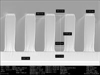
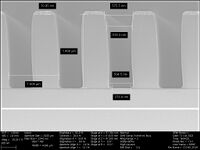
|Not a large effect from adding a little O2 | |||
| | |||
<gallery caption="SiO2 etch with Cr mask on wafer piece on Si carrier 6 min etch, H2:0sccm, O2:5sccm" perrow="6" widths="200px" heights="150px"> | <gallery caption="SiO2 etch with Cr mask on wafer piece on Si carrier 6 min etch, H2:0sccm, O2:5sccm" perrow="6" widths="200px" heights="150px"> | ||
File:C10026_03__05.jpg | File:C10026_03__05.jpg | ||
| Line 117: | Line 180: | ||
File:C10026_03__10.jpg | File:C10026_03__10.jpg | ||
</gallery> | </gallery> | ||
|- style="vertical-align:top;" | |||
| | |||
*Coil Power [W]:2500 | |||
*Platen Power [W]: 200 | |||
*Platen temperature [<sup>o</sup>C]: 20 | |||
*H2 flow [sccm]:0 | |||
*'''O2 flow [sccm]: 0''' | |||
*'''C<sub>4</sub>F<sub>8</sub> flow [sccm]: 13.0''' | |||
*'''He flow [sccm]:225''' | |||
*Pressure:Fully open APC valve ('''3.35 mTorr''') | |||
*Electromagnetic coils (EM) 'outer coil' / 'inner coil':'2 A' / '30 A' | |||
*PLEASE DO NOT RUN WITH THESE SETTINGS FOR MORE THAN 6 MIN | |||
|Reducing total flow rate and thereby the pressure gives less passivation/redeposition. Sidewall roughness not so bad. | |||
| | |||
<gallery caption="SiO2 etch with Cr mask on wafer piece on Si carrier 6 min etch, H2:0sccm, C4F8:13sccm He:225sccm, Pressure:3.35mTorr" perrow="6" widths="200px" heights="150px"> | <gallery caption="SiO2 etch with Cr mask on wafer piece on Si carrier 6 min etch, H2:0sccm, C4F8:13sccm He:225sccm, Pressure:3.35mTorr" perrow="6" widths="200px" heights="150px"> | ||
File:C10082_11.jpg | File:C10082_11.jpg | ||
| Line 125: | Line 201: | ||
File:C10082_03.jpg | File:C10082_03.jpg | ||
File:C10082_01.jpg | File:C10082_01.jpg | ||
File:C010082top_07.jpg | |||
File:C010082top_03.jpg | |||
File:C010082tilt30_13.jpg | |||
</gallery> | </gallery> | ||
|- style="vertical-align:top;" | |||
| | |||
*'''Coil Power [W]:1200''' | |||
*'''Platen Power [W]: 150''' | |||
*Platen temperature [<sup>o</sup>C]: 20 | |||
*H2 flow [sccm]:0 | |||
*O2 flow [sccm]: 0 | |||
*C<sub>4</sub>F<sub>8</sub> flow [sccm]: 13.0 | |||
*He flow [sccm]:225 | |||
*Pressure:Fully open APC valve (3.35 mTorr) | |||
*Electromagnetic coils (EM) 'outer coil' / 'inner coil':'2 A' / '30 A' | |||
*PLEASE DO NOT RUN WITH THESE SETTINGS FOR MORE THAN 6 MIN | |||
|Reducing the coil power a lot and platen power a little gives more sidewall passivation/redeposition | |||
| | |||
<gallery caption="SiO2 etch with Cr mask on wafer piece on Si carrier 6 min etch, H2:0sccm, C4F8:13sccm He:225sccm, Pressure:3.35mTorr; platen power 150W, coil power:1200W" perrow="6" widths="200px" heights="150px"> | <gallery caption="SiO2 etch with Cr mask on wafer piece on Si carrier 6 min etch, H2:0sccm, C4F8:13sccm He:225sccm, Pressure:3.35mTorr; platen power 150W, coil power:1200W" perrow="6" widths="200px" heights="150px"> | ||
File:C10084_15.jpg | File:C10084_15.jpg | ||
| Line 134: | Line 226: | ||
File:C10084_06.jpg | File:C10084_06.jpg | ||
File:C10084_03.jpg | File:C10084_03.jpg | ||
</gallery> | </gallery> | ||
|- style="vertical-align:top;" | |||
| | |||
*Coil Power [W]:1200 | |||
*Platen Power [W]: 150 | |||
*Platen temperature [<sup>o</sup>C]: 20 | |||
*H2 flow [sccm]:0 | |||
*'''O2 flow [sccm]: 10''' | |||
*C<sub>4</sub>F<sub>8</sub> flow [sccm]: 13.0 | |||
*'''He flow [sccm]:215''' | |||
*Pressure:Fully open APC valve (3.35 mTorr) | |||
*Electromagnetic coils (EM) 'outer coil' / 'inner coil':'2 A' / '30 A' | |||
*PLEASE DO NOT RUN WITH THESE SETTINGS FOR MORE THAN 6 MIN | |||
|Adding oxygen reduces the passivation/redeposition | |||
| | |||
<gallery caption="SiO2 etch with Cr mask on wafer piece on Si carrier 6 min etch, H2:0sccm, C4F8:13sccm He:215sccm O2:10sccm, Pressure:3.6mTorr; platen power 150W, coil power:1200W" perrow="6" widths="200px" heights="150px"> | <gallery caption="SiO2 etch with Cr mask on wafer piece on Si carrier 6 min etch, H2:0sccm, C4F8:13sccm He:215sccm O2:10sccm, Pressure:3.6mTorr; platen power 150W, coil power:1200W" perrow="6" widths="200px" heights="150px"> | ||
File:C10093_03__11.jpg | File:C10093_03__11.jpg | ||
| Line 145: | Line 249: | ||
File:C10093_03__01.jpg | File:C10093_03__01.jpg | ||
</gallery> | </gallery> | ||
|- style="vertical-align:top;" | |||
| | |||
*Coil Power [W]:1200 | |||
*Platen Power [W]: 150 | |||
*Platen temperature [<sup>o</sup>C]: 20 | |||
*H2 flow [sccm]:0 | |||
*'''O2 flow [sccm]: 20''' | |||
*C<sub>4</sub>F<sub>8</sub> flow [sccm]: 13.0 | |||
*'''He flow [sccm]:205''' | |||
*Pressure:Fully open APC valve (3.35 mTorr) | |||
*Electromagnetic coils (EM) 'outer coil' / 'inner coil':'2 A' / '30 A' | |||
*PLEASE DO NOT RUN WITH THESE SETTINGS FOR MORE THAN 6 MIN | |||
|Adding more oxygen reduces further the passivation/redeposition but some trenching appears. | |||
| | |||
<gallery caption="SiO2 etch with Cr mask on wafer piece on Si carrier 6 min etch, H2:0sccm, C4F8:13sccm He:205sccm O2:20sccm, Pressure:3.6mTorr; platen power 150W, coil power:1200W" perrow="7" widths="200px" heights="150px"> | <gallery caption="SiO2 etch with Cr mask on wafer piece on Si carrier 6 min etch, H2:0sccm, C4F8:13sccm He:205sccm O2:20sccm, Pressure:3.6mTorr; platen power 150W, coil power:1200W" perrow="7" widths="200px" heights="150px"> | ||
File:C10101_03__12.jpg | File:C10101_03__12.jpg | ||
| Line 155: | Line 272: | ||
File:C10101_03__14.jpg | File:C10101_03__14.jpg | ||
</gallery> | </gallery> | ||
|- style="vertical-align:top;" | |||
| | |||
*'''Coil Power [W]:1800''' | |||
*Platen Power [W]: 150 | |||
*Platen temperature [<sup>o</sup>C]: 20 | |||
*H2 flow [sccm]:0 | |||
*'''O2 flow [sccm]: 10''' | |||
*C<sub>4</sub>F<sub>8</sub> flow [sccm]: 13.0 | |||
*'''He flow [sccm]:215''' | |||
*Pressure:Fully open APC valve (3.35 mTorr) | |||
*Electromagnetic coils (EM) 'outer coil' / 'inner coil':'2 A' / '30 A' | |||
*PLEASE DO NOT RUN WITH THESE SETTINGS FOR MORE THAN 6 MIN | |||
|Increasing coil power reduces trenching but increases passivation/redeposition | |||
| | |||
<gallery caption="SiO2 etch with Cr mask on wafer piece on Si carrier 6 min etch, H2:0sccm, C4F8:13sccm He:215sccm O2:10sccm, Pressure:3.6mTorr; platen power 150W, coil power:1800W" perrow="6" widths="200px" heights="150px"> | <gallery caption="SiO2 etch with Cr mask on wafer piece on Si carrier 6 min etch, H2:0sccm, C4F8:13sccm He:215sccm O2:10sccm, Pressure:3.6mTorr; platen power 150W, coil power:1800W" perrow="6" widths="200px" heights="150px"> | ||
File:C10102_03__05.jpg | File:C10102_03__05.jpg | ||
| Line 164: | Line 294: | ||
File:C10102_03__16.jpg | File:C10102_03__16.jpg | ||
</gallery> | </gallery> | ||
|- style="vertical-align:top;" | |||
| | |||
*Coil Power [W]:1800 | |||
*Platen Power [W]: 150 | |||
*Platen temperature [<sup>o</sup>C]: 20 | |||
*H2 flow [sccm]:0 | |||
*'''O2 flow [sccm]: 20''' | |||
*C<sub>4</sub>F<sub>8</sub> flow [sccm]: 13.0 | |||
*'''He flow [sccm]:205''' | |||
*Pressure:Fully open APC valve (3.6 mTorr) | |||
*Electromagnetic coils (EM) 'outer coil' / 'inner coil':'2 A' / '30 A' | |||
*PLEASE DO NOT RUN WITH THESE SETTINGS FOR MORE THAN 6 MIN | |||
|Adding more O2 reduces the sidewall passivation/redeposition | |||
| | |||
<gallery caption="SiO2 etch with Cr mask on wafer piece on Si carrier 6 min etch, H2:0sccm, C4F8:13sccm He:205sccm O2:20sccm, Pressure:3.6mTorr; platen power 150W, coil power:1800W" perrow="6" widths="200px" heights="150px"> | <gallery caption="SiO2 etch with Cr mask on wafer piece on Si carrier 6 min etch, H2:0sccm, C4F8:13sccm He:205sccm O2:20sccm, Pressure:3.6mTorr; platen power 150W, coil power:1800W" perrow="6" widths="200px" heights="150px"> | ||
File:C10110_04.jpg | File:C10110_04.jpg | ||
| Line 172: | Line 315: | ||
File:C10110_12.jpg | File:C10110_12.jpg | ||
</gallery> | </gallery> | ||
|- style="vertical-align:top;" | |||
| | |||
*'''Coil Power [W]:1200''' | |||
*'''Platen Power [W]: 100''' | |||
*Platen temperature [<sup>o</sup>C]: 20 | |||
*H2 flow [sccm]:0 | |||
*O2 flow [sccm]: 20 | |||
*C<sub>4</sub>F<sub>8</sub> flow [sccm]: 13.0 | |||
*He flow [sccm]:205 | |||
*Pressure:Fully open APC valve (3.6 mTorr) | |||
*Electromagnetic coils (EM) 'outer coil' / 'inner coil':'2 A' / '30 A' | |||
*PLEASE DO NOT RUN WITH THESE SETTINGS FOR MORE THAN 6 MIN | |||
|Running with the lower coil power and reducing the platen power also seems to reduced the sidewall passivatin/redeposition, but etch rate goes down | |||
| | |||
<gallery caption="SiO2 etch with Cr mask on wafer piece on Si carrier 6 min etch, H2:0sccm, C4F8:13sccm He:205sccm O2:20sccm, Pressure:3.6mTorr; platen power 100W, coil power:1200W" perrow="7" widths="200px" heights="150px"> | <gallery caption="SiO2 etch with Cr mask on wafer piece on Si carrier 6 min etch, H2:0sccm, C4F8:13sccm He:205sccm O2:20sccm, Pressure:3.6mTorr; platen power 100W, coil power:1200W" perrow="7" widths="200px" heights="150px"> | ||
File:C10119_01.jpg | File:C10119_01.jpg | ||
| Line 181: | Line 337: | ||
File:C10119_11.jpg | File:C10119_11.jpg | ||
</gallery> | </gallery> | ||
|- style="vertical-align:top;" | |||
<gallery caption="SiO2 etch with Cr mask on wafer piece on Si carrier 14 min etch (PLEASE DO NOT REPEAT THIS LONG TIME), H2:0sccm, C4F8:13sccm He:205sccm O2:20sccm, Pressure:3.6mTorr; platen power 100W, coil power:1200W" perrow="7" widths="200px" heights="150px"> | | | ||
*Coil Power [W]:1200 | |||
*Platen Power [W]: 100 | |||
*Platen temperature [<sup>o</sup>C]: 20 | |||
*H2 flow [sccm]:0 | |||
*O2 flow [sccm]: 20 | |||
*C<sub>4</sub>F<sub>8</sub> flow [sccm]: 13.0 | |||
*He flow [sccm]:205 | |||
*Pressure:Fully open APC valve (3.6 mTorr) | |||
*Electromagnetic coils (EM) 'outer coil' / 'inner coil':'2 A' / '30 A' | |||
*PLEASE DO NOT RUN WITH THESE SETTINGS FOR MORE THAN 6 MIN | |||
|Repeating with longer etch time to etch 1500 nm down. Unfortunately this damaged the hardware due to the EM coils getting too hot. | |||
| | |||
<gallery caption="SiO2 etch with Cr mask on wafer piece on Si carrier '''14 min etch''' (PLEASE DO NOT REPEAT THIS LONG TIME), H2:0sccm, C4F8:13sccm He:205sccm O2:20sccm, Pressure:3.6mTorr; platen power 100W, coil power:1200W" perrow="7" widths="200px" heights="150px"> | |||
File:C10160_02.jpg | File:C10160_02.jpg | ||
File:C10160_06.jpg | File:C10160_06.jpg | ||
| Line 191: | Line 360: | ||
File:Contour Plot Y32 EM_02_30 blue to red.jpg| Etch on none patterned wafer, Uniformity: +- 6.4% | File:Contour Plot Y32 EM_02_30 blue to red.jpg| Etch on none patterned wafer, Uniformity: +- 6.4% | ||
</gallery> | </gallery> | ||
|- style="vertical-align:top;" | |||
<gallery caption="SiO2 etch with Cr mask on wafer piece on Si carrier 10 min etch, H2:0sccm, C4F8:13sccm He:205sccm O2:20sccm, Pressure:3.6mTorr; platen power 150W, coil power:1800W" perrow="6" widths="200px" heights="150px"> | | | ||
*'''Coil Power [W]:1800''' | |||
*'''Platen Power [W]: 150''' | |||
*Platen temperature [<sup>o</sup>C]: 20 | |||
*H2 flow [sccm]:0 | |||
*O2 flow [sccm]: 20 | |||
*C<sub>4</sub>F<sub>8</sub> flow [sccm]: 13.0 | |||
*He flow [sccm]:205 | |||
*Pressure:Fully open APC valve (3.6 mTorr) | |||
*Electromagnetic coils (EM) 'outer coil' / 'inner coil':'2 A' / '30 A' | |||
*PLEASE DO NOT RUN WITH THESE SETTINGS FOR MORE THAN 6 MIN | |||
|Running 1800W/150W at increased time to etch down to 1500 nm. | |||
| | |||
<gallery caption="C10161 SiO2 etch with Cr mask on wafer piece on Si carrier '''10 min etch''', H2:0sccm, C4F8:13sccm He:205sccm O2:20sccm, Pressure:3.6mTorr; platen power 150W, coil power:1800W" perrow="6" widths="200px" heights="150px"> | |||
File:C10161_01.jpg | File:C10161_01.jpg | ||
File:C10161_03.jpg | File:C10161_03.jpg | ||
| Line 199: | Line 381: | ||
File:C10161_09.jpg | File:C10161_09.jpg | ||
File:C10161_11.jpg | File:C10161_11.jpg | ||
File:C010161top_01.jpg | |||
File:C010161tilt_04.jpg | |||
</gallery> | </gallery> | ||
|- style="vertical-align:top;" | |||
<gallery caption="SiO2 etch with Cr mask on wafer piece on Si carrier 14 min etch, EM:0/0 H2:0sccm, C4F8:13sccm He:205sccm O2:20sccm, Pressure:3.9mTorr; platen power 100W, coil power:1200W | | | ||
*'''Coil Power [W]:1200''' | |||
*'''Platen Power [W]: 100''' | |||
*Platen temperature [<sup>o</sup>C]: 20 | |||
*H2 flow [sccm]:0 | |||
*O2 flow [sccm]: 20 | |||
*C<sub>4</sub>F<sub>8</sub> flow [sccm]: 13.0 | |||
*He flow [sccm]:205 | |||
*Pressure:Fully open APC valve (3.9 mTorr) | |||
*'''Electromagnetic coils (EM) 'outer coil' / 'inner coil':'0 A' / '0 A'''' | |||
|Repeating the 1200W/100W recipes at 14 min but without the EM coils. For this recipe the uniformity over the wafer improved from removing the EM coils, so no need for those and now the recipe could run 14 min without damaging the hardware. The profile looked as before. After removing the Cr I looked from the top and with a tilted view and saw the the sidewall roughness was very bad. | |||
| | |||
<gallery perrow="7" widths="200px" heights="150px" caption="C10184: SiO2 etch with Cr mask on wafer piece on Si carrier 14 min etch, EM:0/0 H2:0sccm, C4F8:13sccm He:205sccm O2:20sccm, Pressure:3.9mTorr; platen power 100W, coil power:1200W"> | |||
File:C10184_01.jpg | File:C10184_01.jpg | ||
File:C10184_05.jpg | File:C10184_05.jpg | ||
| Line 209: | Line 405: | ||
File:C10184_12.jpg | File:C10184_12.jpg | ||
File:Contour Plot Y33 EM_0_0 blue to red.jpg| Etch on none patterned wafer, Uniformity: +-1.7% | File:Contour Plot Y33 EM_0_0 blue to red.jpg| Etch on none patterned wafer, Uniformity: +-1.7% | ||
File:C010184top_01.jpg | |||
File:C010184top_04.jpg | |||
File:C010184tilt30plasmaO2_02.jpg| tilt 30 degrees | |||
File:C010184tilt30plasmaO2_01.jpg| tilt 30 degrees | |||
File:C010184tilt20plasmaO2_07.jpg| tilt 20 degrees | |||
File:C010184tilt20plasmaO2_05.jpg| tilt 20 degrees | |||
File:C1018405.jpg|After RCA clean | |||
File:C1018402.jpg|After RCA clean | |||
File:C1018403.jpg|After RCA clean | |||
</gallery> | |||
|- style="vertical-align:top;" | |||
| | |||
*'''Coil Power [W]:2500''' | |||
*Platen Power [W]: 100 | |||
*Platen temperature [<sup>o</sup>C]: 20 | |||
*H2 flow [sccm]:0 | |||
*O2 flow [sccm]: 20 | |||
*C<sub>4</sub>F<sub>8</sub> flow [sccm]: 13.0 | |||
*He flow [sccm]:205 | |||
*Pressure:Fully open APC valve (3.9 mTorr) | |||
*Electromagnetic coils (EM) 'outer coil' / 'inner coil':'0 A' / '0 A' | |||
|Tried high coil power and low platen power. This seemed to give som undercutting,especially on the narrow lines. The smallest has been etched away. The etch rate was very low | |||
| | |||
<gallery caption="SiO2 etch with Cr mask on wafer piece on Si carrier 14 min etch, EM:0/0 H2:0sccm, C4F8:13sccm He:205sccm O2:20sccm, Pressure:3.9mTorr; platen power 100W, coil power:2500W" perrow="7" widths="200px" heights="150px"> | |||
File:C10381_04.jpg | |||
File:C10381_06.jpg | |||
File:C10381_07.jpg | |||
File:C10381_30dg_17.jpg | |||
File:C10381_30dg_21.jpg | |||
</gallery> | |||
|- style="vertical-align:top;" | |||
| | |||
*Coil Power [W]:2500 | |||
*'''Platen Power [W]: 200''' | |||
*Platen temperature [<sup>o</sup>C]: 20 | |||
*H2 flow [sccm]:0 | |||
*'''O2 flow [sccm]: 0''' | |||
*C<sub>4</sub>F<sub>8</sub> flow [sccm]: 13.0 | |||
*He flow [sccm]:225 | |||
*Pressure:Fully open APC valve (3.9 mTorr) | |||
*Electromagnetic coils (EM) 'outer coil' / 'inner coil':'0 A' / '0 A' | |||
|Increasing the platen power and and removing the oxygen helped on the under cutting but the lines are still very narrow at the bottom. It also increased the etch rate | |||
| | |||
<gallery caption="SiO2 etch with Cr mask on wafer piece on Si carrier 14 min etch, EM:0/0 H2:0sccm, C4F8:13sccm He:225sccm O2:0sccm, Pressure:3.9mTorr; platen power 200W, coil power:2500W" perrow="7" widths="200px" heights="150px"> | |||
File:C10393_04.jpg | |||
File:C10393_06.jpg | |||
File:C10393_09.jpg | |||
File:C10393_11.jpg | |||
File:C10393_12.jpg | |||
File:C10393_14.jpg | |||
File:C10393_16.jpg | |||
</gallery> | |||
|- style="vertical-align:top;" | |||
| | |||
*'''14 min''' | |||
*Coil Power [W]:2500 | |||
*Platen Power [W]: 200 | |||
*Platen temperature [<sup>o</sup>C]: 20 | |||
*H2 flow [sccm]:0 | |||
*O2 flow [sccm]: 20 | |||
*C<sub>4</sub>F<sub>8</sub> flow [sccm]: 13.0 | |||
*He flow [sccm]:205 | |||
*Pressure:Fully open APC valve (3.9 mTorr) | |||
*Electromagnetic coils (EM) 'outer coil' / 'inner coil':'0 A' / '0 A' | |||
|Adding the oxygen again further increased the etch rate and reduced the CD (Critical Dimension) of the Cr mask. | |||
| | |||
<gallery caption="SiO2 etch with Cr mask on wafer piece on Si carrier 14 min etch, EM:0/0 H2:0sccm, C4F8:13sccm He:205sccm O2:20sccm, Pressure:3.9mTorr; platen power 200W, coil power:2500W" perrow="7" widths="200px" heights="150px"> | |||
File:C10399_01.jpg | |||
File:C10399_02.jpg | |||
File:C10399_04.jpg | |||
File:C10399_08.jpg | |||
File:C10399_10.jpg | |||
File:C10399_13.jpg | |||
</gallery> | |||
|- style="vertical-align:top;" | |||
| | |||
*'''Back to start setting without EM coils - 14 min''' | |||
*Coil Power [W]:2500 | |||
*Platen Power [W]: 200 | |||
*Platen temperature [<sup>o</sup>C]: 20 | |||
*H2 flow [sccm]:25.6 | |||
*O2 flow [sccm]: 0 | |||
*C<sub>4</sub>F<sub>8</sub> flow [sccm]: 25.6 | |||
*He flow [sccm]:448.7 | |||
*Pressure:Fully open APC valve (8-9 mTorr) | |||
*Electromagnetic coils (EM) 'outer coil' / 'inner coil':'0 A' / '0 A' | |||
|I repeated the start setting but without the EM coils. This gives a very none uniform etch over the wafer where in some parts it deposites instead of etching. The profile of 800 nm oitch look fairly good but a closer look reveals the the sidewall is very rough from either redeposition or polymerization. this cannot be removed with a O2 plasma. | |||
| | |||
<gallery caption="SiO2 etch with Cr mask on wafer piece on Si carrier 14 min etch, EM:0/0" perrow="7" widths="200px" heights="150px"> | |||
File:C10576_02.jpg | |||
File:C10576_01.jpg | |||
File:C10576_04.jpg | |||
File:C10576_06.jpg | |||
File:C10576_08.jpg | |||
File:C10576_10.jpg | |||
File:C10576_19.jpg | |||
File:C10576_22.jpg | |||
File:C10576_17.jpg | |||
</gallery> | |||
|- style="vertical-align:top;" | |||
| | |||
*'''Coil Power [W]:600''' | |||
*'''Platen Power [W]: 50''' | |||
*Platen temperature [<sup>o</sup>C]: 20 | |||
*H2 flow [sccm]:0 | |||
*'''O2 flow [sccm]: 10''' | |||
*'''C<sub>4</sub>F<sub>8</sub> flow [sccm]: 6.5''' | |||
*'''He flow [sccm]:100''' | |||
*Pressure:Fully open APC valve ('''<2 mTorr''') | |||
*Electromagnetic coils (EM) 'outer coil' / 'inner coil':'0 A' / '0 A' | |||
|Due to the large sidewall roughness I decided to try and run at lower powers because it looked at some images like an ionbonbardment effect. First try with 600W/50W. The profile looks fairly good but still with some sidewall roughness. there is also some trenching and the Cr mask looks has a facet all the way down to the SiO2. The is also some bowing. | |||
| | |||
<gallery caption=" C10751: SiO2 etch with Cr mask on wafer piece on Si carrier 20 min etch, EM:0/0 H2:0sccm, C4F8:6.5sccm He:100sccm O2:10sccm, Pressure:?mTorr; platen power 50W, coil power:600W" perrow="7" widths="200px" heights="150px"> | |||
File:C10751_02.jpg | |||
File:C10751_05.jpg | |||
File:C10751_07.jpg | |||
File:C10751_09.jpg | |||
File:C10751_11.jpg | |||
File:C10751_12.jpg | |||
</gallery> | |||
|- style="vertical-align:top;" | |||
| | |||
*'''Coil Power [W]:300''' | |||
*'''Platen Power [W]: 25''' | |||
*Platen temperature [<sup>o</sup>C]: 20 | |||
*H2 flow [sccm]:0 | |||
*O2 flow [sccm]: 10 | |||
*C<sub>4</sub>F<sub>8</sub> flow [sccm]: 6.5 | |||
*He flow [sccm]:100 | |||
*Pressure:Fully open APC valve (<2 mTorr) | |||
*Electromagnetic coils (EM) 'outer coil' / 'inner coil':'0 A' / '0 A' | |||
|Even lower powers: 300W/25W. The profiles looks better with less roughness but also mush slower etch rate, so not as deep as the previous. | |||
| | |||
<gallery caption=" C10752: SiO2 etch with Cr mask on wafer piece on Si carrier 30 min etch, EM:0/0 H2:0sccm, C4F8:6.5sccm He:100sccm O2:10sccm, Pressure:?mTorr; platen power 25W, coil power:300W" perrow="6" widths="200px" heights="150px"> | |||
File:C10752_01.jpg | |||
File:C10752_03.jpg | |||
File:C10752_05.jpg | |||
File:C10752_07.jpg | |||
File:C10752_09.jpg | |||
File:C10752_10.jpg | |||
</gallery> | </gallery> | ||
|- style="vertical-align:top;" | |||
| | |||
*'''45 min''' | |||
*Coil Power [W]:300 | |||
*Platen Power [W]: 25 | |||
*Platen temperature [<sup>o</sup>C]: 20 | |||
*H2 flow [sccm]:0 | |||
*O2 flow [sccm]: 10 | |||
*C<sub>4</sub>F<sub>8</sub> flow [sccm]: 6.5 | |||
*He flow [sccm]:100 | |||
*Pressure:Fully open APC valve (<2 mTorr) | |||
*Electromagnetic coils (EM) 'outer coil' / 'inner coil':'0 A' / '0 A' | |||
|Repeating with longer etch time. Low sidewall roughness, less faceting of the Cr mask. Still some trenching and bowing or negative tapering of the profile. | |||
| | |||
<gallery caption=" C10834: SiO2 etch with Cr mask on wafer piece on Si carrier 45 min etch, EM:0/0 H2:0sccm, C4F8:6.5sccm He:100sccm O2:10sccm, Pressure:?mTorr; platen power 25W, coil power:300W" perrow="6" widths="200px" heights="150px"> | |||
File:C10834_12.jpg | |||
File:C10834_10.jpg | |||
File:C10834_08.jpg | |||
File:C10834_06.jpg | |||
File:C10834_02.jpg | |||
File:C10834_04.jpg | |||
File:C10834T_17.jpg | |||
File:C10834T_15.jpg | |||
File:C10834T_20.jpg | |||
File:C10834T_19.jpg | |||
File:C10834T_21.jpg | |||
File:C10834T_22.jpg | |||
</gallery> | |||
|- style="vertical-align:top;" | |||
| | |||
*Coil Power [W]:300 | |||
*'''Platen Power [W]: 20''' | |||
*Platen temperature [<sup>o</sup>C]: 20 | |||
*H2 flow [sccm]:0 | |||
*O2 flow [sccm]: 10 | |||
*C<sub>4</sub>F<sub>8</sub> flow [sccm]: 6.5 | |||
*He flow [sccm]:100 | |||
*Pressure:Fully open APC valve (<2 mTorr) | |||
*Electromagnetic coils (EM) 'outer coil' / 'inner coil':'0 A' / '0 A' | |||
|Decreased the platen power a little to see if this could remove the trenching. Not much different from the last. | |||
| | |||
<gallery caption=" C10844: SiO2 etch with Cr mask on wafer piece on Si carrier 50 min etch, EM:0/0 H2:0sccm, C4F8:6.5sccm He:100sccm O2:10sccm, Pressure:?mTorr; platen power 20W, coil power:300W" perrow="6" widths="200px" heights="150px"> | |||
File:C10844_02.jpg | |||
File:C10844_05.jpg | |||
File:C10844_09.jpg | |||
File:C10844_07.jpg | |||
File:C10844_11.jpg | |||
File:C10844_13.jpg | |||
</gallery> | |||
|} | |||
TEST: | |||
[[File:C12332_06.jpg|400px]] | |||
Latest revision as of 14:54, 29 October 2024
Feedback to this page: click here
Unless otherwise stated, all content in this section was done by Berit Herstrøm, DTU Nanolab
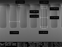
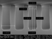
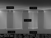
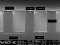
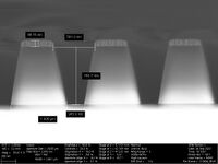
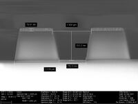
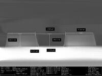
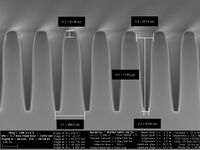
SiO2 trench etching with Cr mask
| Start parameters, variations noted in the gallery headline | Recipe name: no 10 with lower platen power |
|---|---|
| Coil Power [W] | 2500 |
| Platen Power [W] | 200 |
| Platen temperature [oC] | 20 |
| H2 flow [sccm] | 25.6 |
| C4F8 flow [sccm] | 25.6 |
| He flow [sccm] | 448.7 |
| Pressure | Fully open APC valve (8-9 mTorr) |
| Electromagnetic coils (EM) 'outer coil' / 'inner coil' | '2 A' / '30 A' (PLEASE DO NOT RUN WITH THESE SETTINGS FOR MORE THAN 6 MIN) |
- 100 nm Cr mask etched in ICP metal with 500nm DUV neg resist (NUV 2300-0.5) and 65 nm barc.
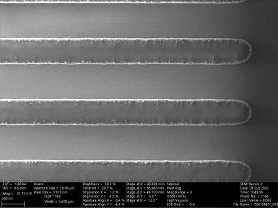
Results
| Temporary conclusions on how the process parameters affect the results in this study: | What process parameters affect the results? |
|
|
Profile SEM images
| Recipe settings | Comments | SEM gallery |
|---|---|---|
|
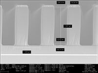
text |
|
|
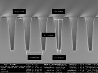
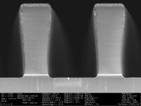
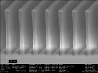
More sidewall passivation on chip than on full wafer |
|
|
Less sidewall passivation from removing the H2 |
|
|
Not a large effect from adding a little O2 |
|
|
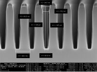
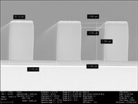
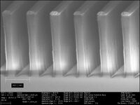
Reducing total flow rate and thereby the pressure gives less passivation/redeposition. Sidewall roughness not so bad. |
|
|
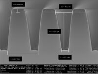
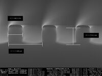
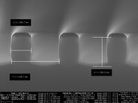
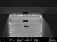
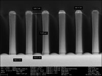
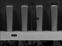
Reducing the coil power a lot and platen power a little gives more sidewall passivation/redeposition |
|
|
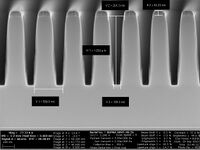
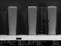
Adding oxygen reduces the passivation/redeposition |
|
|
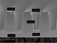
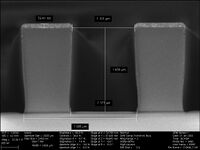
Adding more oxygen reduces further the passivation/redeposition but some trenching appears. |
|
|
Increasing coil power reduces trenching but increases passivation/redeposition |
|
|
Adding more O2 reduces the sidewall passivation/redeposition |
|
|
Running with the lower coil power and reducing the platen power also seems to reduced the sidewall passivatin/redeposition, but etch rate goes down |
|
|
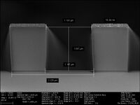
Repeating with longer etch time to etch 1500 nm down. Unfortunately this damaged the hardware due to the EM coils getting too hot. |
|
|
Running 1800W/150W at increased time to etch down to 1500 nm. |
|
|
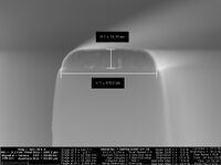
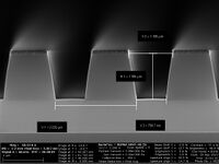
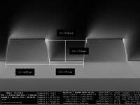
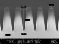
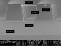
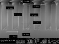
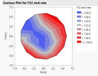
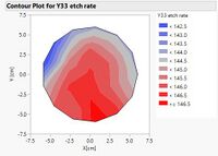
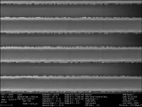
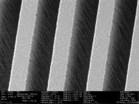
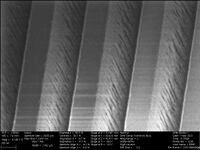
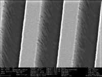
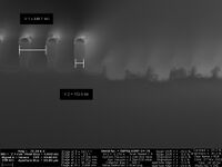
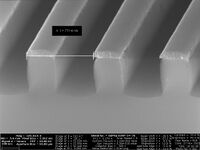
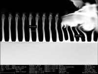
Repeating the 1200W/100W recipes at 14 min but without the EM coils. For this recipe the uniformity over the wafer improved from removing the EM coils, so no need for those and now the recipe could run 14 min without damaging the hardware. The profile looked as before. After removing the Cr I looked from the top and with a tilted view and saw the the sidewall roughness was very bad. |
|
|
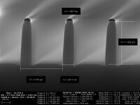
Tried high coil power and low platen power. This seemed to give som undercutting,especially on the narrow lines. The smallest has been etched away. The etch rate was very low |
|
|
Increasing the platen power and and removing the oxygen helped on the under cutting but the lines are still very narrow at the bottom. It also increased the etch rate |
|
|
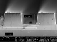
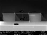
Adding the oxygen again further increased the etch rate and reduced the CD (Critical Dimension) of the Cr mask. |
|
|
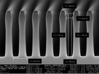
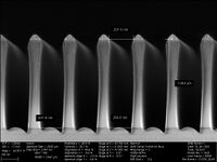
I repeated the start setting but without the EM coils. This gives a very none uniform etch over the wafer where in some parts it deposites instead of etching. The profile of 800 nm oitch look fairly good but a closer look reveals the the sidewall is very rough from either redeposition or polymerization. this cannot be removed with a O2 plasma. |
|
|
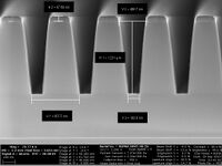
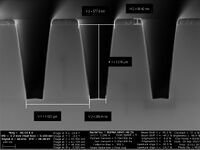
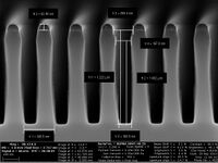
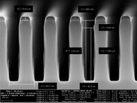
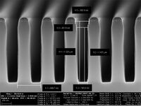
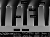
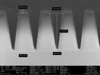
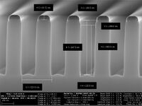
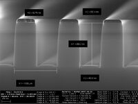
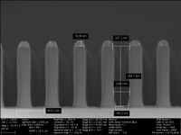
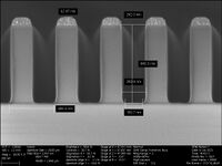
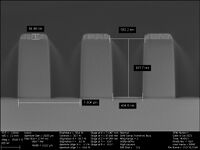
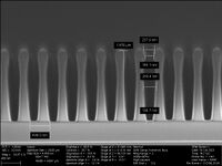
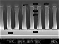
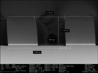
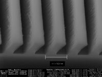
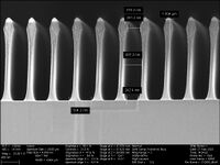
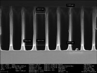
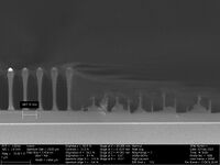
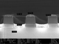
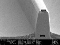
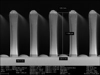
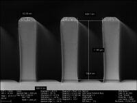
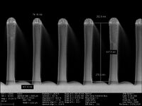
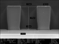
Due to the large sidewall roughness I decided to try and run at lower powers because it looked at some images like an ionbonbardment effect. First try with 600W/50W. The profile looks fairly good but still with some sidewall roughness. there is also some trenching and the Cr mask looks has a facet all the way down to the SiO2. The is also some bowing. |
|
|
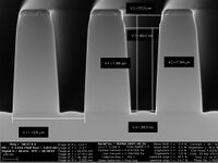
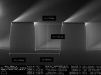
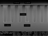
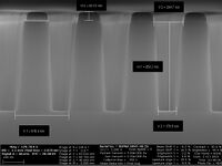
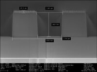
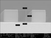
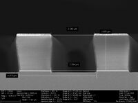
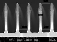
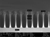
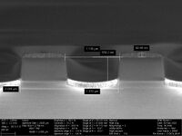
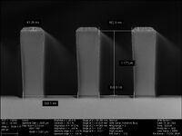
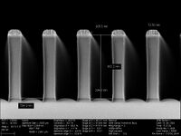
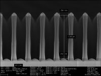
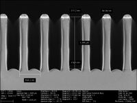
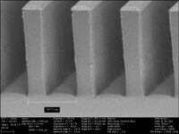
Even lower powers: 300W/25W. The profiles looks better with less roughness but also mush slower etch rate, so not as deep as the previous. |
|
|
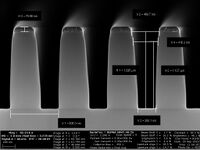
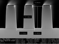
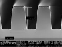
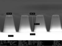
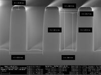
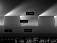
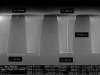
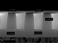
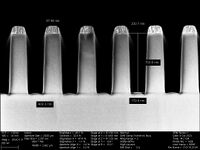
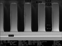
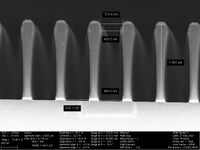
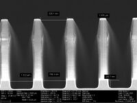
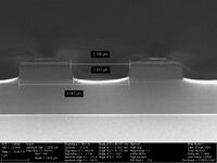
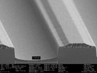
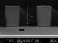
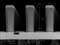
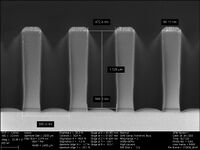
Repeating with longer etch time. Low sidewall roughness, less faceting of the Cr mask. Still some trenching and bowing or negative tapering of the profile. |
|
|
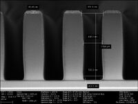
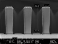
Decreased the platen power a little to see if this could remove the trenching. Not much different from the last. |
|

