Specific Process Knowledge/Lithography/EBeamLithography/Cassettes: Difference between revisions
| (30 intermediate revisions by the same user not shown) | |||
| Line 20: | Line 20: | ||
{| style="border: none; border-spacing: 0; margin: 1em auto; text-align: center;" | {| style="border: none; border-spacing: 0; margin: 1em auto; text-align: center;" | ||
|- | |- | ||
| [[image:BSPCL-520.png| | | [[image:BSPCL-520.png|1000px]] | ||
|- | |- | ||
| colspan="1" style="text-align:center;| | | colspan="1" style="text-align:center;| | ||
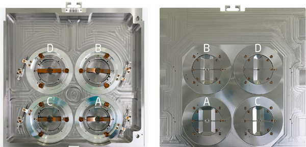
Back side (left )and front side view (right) of the 4" wafer titanium cassette (BSPCL-520). | Back side (left )and front side view (right) of the 4" wafer titanium cassette (BSPCL-520). | ||
|} | |||
== Stage position and cassette orientation== | |||
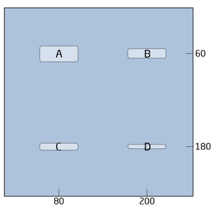
The stage control window indicates where the stage is currently placed. It indicates this position with a coordinate and a small, red indicator inside the blue box, as illustrated below. Sadly, the system does not indicate how the cassette or cassette slots are placed, thus we have provided an approximate illustration of this below. This can be used as a sanity check to verify that the system is working on the correct cassette slot. In the example below, slot A of the chips cassette is being exposed. Similar illustrations for other cassettes are provided in the cassettes overview table further down this page. | |||
{| style="border: none; border-spacing: 0; margin: 1em auto; text-align: center;" | |||
|- | |||
| [[image:StageControlWindow.png|500px]] || [[image:StagePos.png|400px]] | |||
|- | |||
| colspan="2" style="text-align:enter;| | |||
Left: The stage position is indicated by the red dot inside the blue square. Right: Example of cassette and slot placement relative to the blue square in the Stage Control Window. | |||
|} | |} | ||
| Line 46: | Line 57: | ||
The substrate must overlap at least 0.5 mm on both sides of the slot. Hence the height of a chip must be at least 1 mm larger than the slot height, i.e. in order to use slot 3B the chip height must be at least 13.0 mm. | The substrate must overlap at least 0.5 mm on both sides of the slot. Hence the height of a chip must be at least 1 mm larger than the slot height, i.e. in order to use slot 3B the chip height must be at least 13.0 mm. | ||
As the smaller slots are quite narrow and suffer from a significant y-axis offset, it can be necessary to apply an offset for correct placement. The offset indicated below is the observed offset, hence to counter it one must apply a y-axis offset in the opposite direction. | |||
==Wafer exposable area== | |||
As the wafer is clamped to the cassette a small portion along the circumference is covered by the cassette and hence this part is not exposable. The exposable diameter for round wafers are: | |||
*2": 44 mm | |||
*4": 93 mm | |||
*6": 138 mm | |||
== Cassette overview == | == Cassette overview == | ||
The table below provides details on all available cassettes. | |||
Users of the chip cassettes should notice that there is a significant y-axis offset between the slot center positions and the actual stage position. The measured offsets are indicated in the table. As seen, they are all negative and hence users should apply a positive y-axis offset in order to get the pattern exposed correctly in the center of the slot/substrate. | |||
There is also a minor shift between the pre-aligner coordinates and the actual stage coordinates. These are indicated in the last column. In order to hit the alignment mark on the first scan users should add this offset to the P-mark offset found on the pre-aligner. | |||
{| class="wikitable" | {| class="wikitable" | ||
|+ Cassette overview | |+ Cassette overview | ||
|- | |- | ||
! Substrate size !! ID !! Slot ID !! Material !! Image !! | ! Substrate size !! ID !! Slot ID !! Material !! Image !! Position indication !! Approximate offset [µm] !! PA to stage shift [µm] | ||
|- | |- | ||
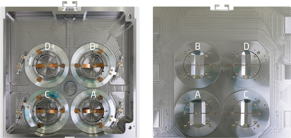
| Chips || BM4P-509 || 3A, 3B, 3C, 3D || Ti || [[image:BM4P-509_cas.png| | | Chips || BM4P-509 || 3A, 3B, 3C, 3D || Ti || [[image:BM4P-509_cas.png|600px]] || [[image:BM4P-509 small.png|300px]] | ||
|| 3A: -810 µm | |||
|| | |||
3A: -810 µm | |||
3B: -780 µm | 3B: -780 µm | ||
| Line 68: | Line 86: | ||
3C: -840 µm | 3C: -840 µm | ||
3D: -975 µm | 3D: -975 µm | ||
|| | |||
|- | |- | ||
| Chips || BM4P-510 || 3A, 3B, 3C, 3D || Ti || [[image:BM4P-510_cas.png| | | Chips || BM4P-510 || 3A, 3B, 3C, 3D || Ti || [[image:BM4P-510_cas.png|600px]] || [[image:BM4P-509 small.png|300px]] || | ||
|- | |- | ||
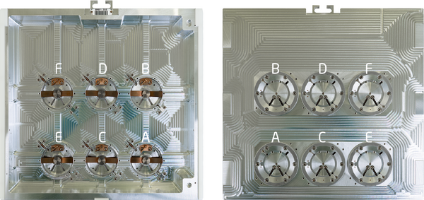
| 2" || BM6P-006 || 2A, 2B, 2C, 2D, 2E, 2F || Al || [[image:BM6P-006_cas.png| | | 2" || BM6P-006 || 2A, 2B, 2C, 2D, 2E, 2F || Al || [[image:BM6P-006_cas.png|600px]] || [[image:BM6P-502 small.png|300px]] || | ||
|- | |- | ||
| 2" || BM6P-502 || 2A, 2B, 2C, 2D, 2E, 2F || Ti || [[image:BM6P-502_cas.png| | | 2" || BM6P-502 || 2A, 2B, 2C, 2D, 2E, 2F || Ti || [[image:BM6P-502_cas.png|600px]] || [[image:BM6P-502 small.png|300px]] || | ||
|- | |- | ||
| 3" || BM4P-021 || 3A, 3B, 3C, 3D || Al || [[image:BM4P-021_cas.png| | | 3" || BM4P-021 || 3A, 3B, 3C, 3D || Al || [[image:BM4P-021_cas.png|600px]] || [[image:BM4P-509 small copy.png|300px]] || | ||
|- | |- | ||
| 3" || BM4P-025 || 3A, 3B, 3C, 3D || Al || [[image:BM4P-025_cas.png| | | 3" || BM4P-025 || 3A, 3B, 3C, 3D || Al || [[image:BM4P-025_cas.png|600px]] || [[image:BM4P-509 small copy.png|300px]] || | ||
|- | |- | ||
| 4" || BSPCL-520 || 4A, 4B, 4C || Ti || [[image:BSPCL-520_cas.png| | | 4" || BSPCL-520 || 4A, 4B, 4C || Ti || [[image:BSPCL-520_cas.png|600px]] || [[image:BSPCL-520 small.png|300px]] || | ||
|- | |- | ||
| 4" || BM2P-011 || 4D, 4E || Al || [[image:BM2P-011_cas.png| | | 4" || BM2P-011 || 4D, 4E || Al || [[image:BM2P-011_cas.png|600px]] || [[image:BM2P-011 small.png|300px]] || || 4D: (330,150) | ||
|- | |- | ||
| 6" || BW6-009 || 6A || Al || [[image:BW6-009.png| | | 6" || BW6-009 || 6A || Al || [[image:BW6-009.png|600px]] || [[image:BW6-009 small.png|300px]] || | ||
|- | |- | ||
| 6" || BW6-042 || 6A || Al || [[image:BW6-042_cas.png| | | 6" || BW6-042 || 6A || Al || [[image:BW6-042_cas.png|600px]] || [[image:BW6-009 small.png|300px]] || | ||
|- | |- | ||
| 8" || BSPCL-514 || 8A || Ti || [[image:BPSPCL-514_cas.png| | | 8" || BSPCL-514 || 8A || Ti || [[image:BPSPCL-514_cas.png|600px]] || [[image:BW6-009 small.png|300px]] || | ||
|- | |- | ||
| Mask || B6025-025 || || Ti || [[image:B6025-025.png| | | Mask || B6025-025 || || Ti || [[image:B6025-025.png|600px]] || (140.000, 120.000) || | ||
|} | |} | ||
Latest revision as of 10:56, 17 September 2024
Feedback to this page: click here
Content and illustration by Thomas Pedersen, DTU Nanolab unless otherwise noted.
JEOL 9500 cassette specifications page
General information
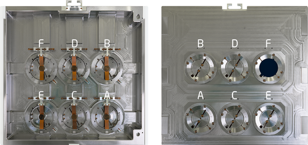
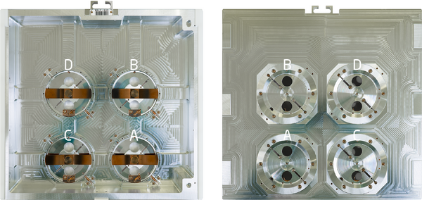
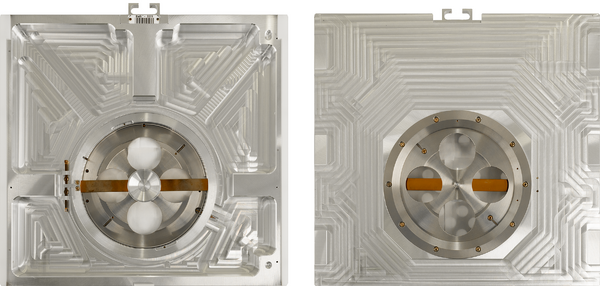
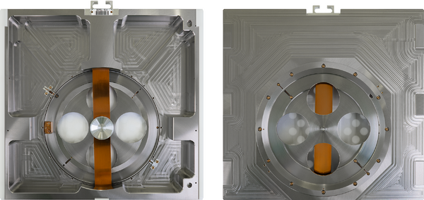
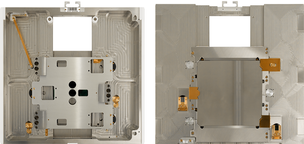
Wafer cassettes are available for 2", 4", 6" and 8" wafers. Wafers must be intact, i.e. fractions of wafers can not be exposed in these cassettes. Cassettes dedicated chip exposure are also available. While cassettes are individually adapted to a specific substrate type they naturally share a set of features as illustrated below.
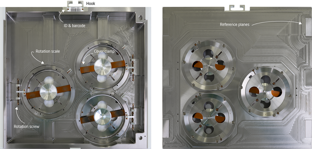
- The front side has six reference planes. One should avoid touching these to preserver them as clean and scratch free as possible.
- One should also avoid touching the hook.
- On the back side each cassettes has a unique ID and barcode. The barcode is read by the cassette transfer system.
- Substrates are held in place by a cover ring that locks with a copper spring clamp. To unlock a cover simply press down on the copper clamp and turn to the open position.
- Most cassettes have a set screw that can be used to precisely rotate the entire substrate slot. This is mostly used for alignment on the pre-aligner.
- Cassettes with a rotation set screw also has a rotation scale.
- Some cassettes have engraved slot ID's
Cassettes are either made in aluminium or titanium. The thermal expansion coefficient of titanium is about one third of that of aluminium. Hence thermal drift is reduced on titanium cassettes.
|
|
Back side (left )and front side view (right) of the 4" wafer titanium cassette (BSPCL-520). |
Stage position and cassette orientation
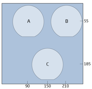
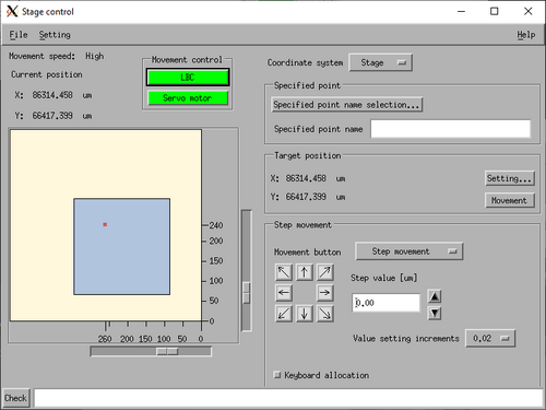
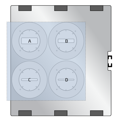
The stage control window indicates where the stage is currently placed. It indicates this position with a coordinate and a small, red indicator inside the blue box, as illustrated below. Sadly, the system does not indicate how the cassette or cassette slots are placed, thus we have provided an approximate illustration of this below. This can be used as a sanity check to verify that the system is working on the correct cassette slot. In the example below, slot A of the chips cassette is being exposed. Similar illustrations for other cassettes are provided in the cassettes overview table further down this page.
 |
|
|
Left: The stage position is indicated by the red dot inside the blue square. Right: Example of cassette and slot placement relative to the blue square in the Stage Control Window. | |
Coordinate system
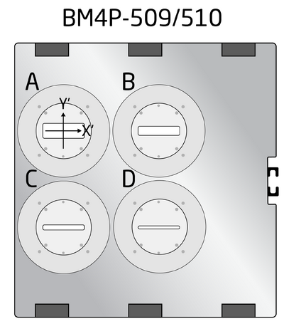
When placing a substrate in a cassette it is essential to know the relation between the cassette coordinate system and the design coordinate system. On wafer cassettes this is very obvious as they have a flat pin where the flat of the wafer will sit. On chip cassettes the substrate can however be placed at any rotation and hence the exposed pattern can end up upside down if one does not pay attention to this. The pattern coordinate system x' and y' is illustrated below. Notice that the is when the cassette is viewed from the front side with the hook placed to the right.
|
|
Coordinate system is regular orientation when cassette is viewed from the front and hook placed to the right. |
Chip cassette slot dimensions
The slots on chip cassettes are in all cases 70 mm wide. The height of the slots are slot dependent and are:
- 3A: 20 mm
- 3B: 12 mm
- 3C: 8 mm
- 3D: 4 mm
The substrate must overlap at least 0.5 mm on both sides of the slot. Hence the height of a chip must be at least 1 mm larger than the slot height, i.e. in order to use slot 3B the chip height must be at least 13.0 mm.
As the smaller slots are quite narrow and suffer from a significant y-axis offset, it can be necessary to apply an offset for correct placement. The offset indicated below is the observed offset, hence to counter it one must apply a y-axis offset in the opposite direction.
Wafer exposable area
As the wafer is clamped to the cassette a small portion along the circumference is covered by the cassette and hence this part is not exposable. The exposable diameter for round wafers are:
- 2": 44 mm
- 4": 93 mm
- 6": 138 mm
Cassette overview
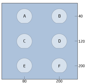
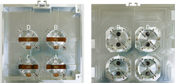
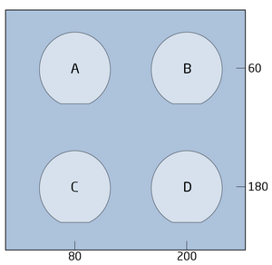
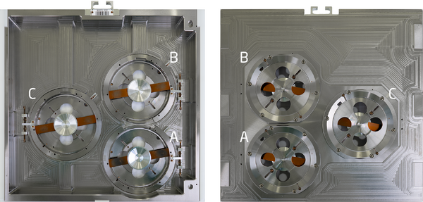
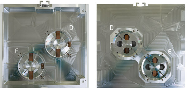
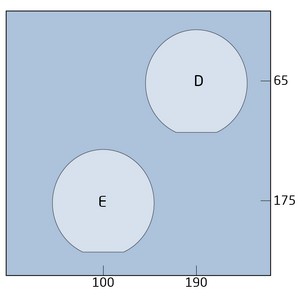
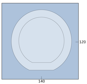
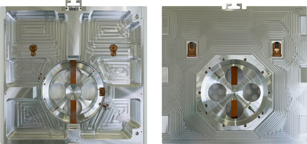
The table below provides details on all available cassettes.
Users of the chip cassettes should notice that there is a significant y-axis offset between the slot center positions and the actual stage position. The measured offsets are indicated in the table. As seen, they are all negative and hence users should apply a positive y-axis offset in order to get the pattern exposed correctly in the center of the slot/substrate.
There is also a minor shift between the pre-aligner coordinates and the actual stage coordinates. These are indicated in the last column. In order to hit the alignment mark on the first scan users should add this offset to the P-mark offset found on the pre-aligner.

