Specific Process Knowledge/Etch/DRIE-Pegasus/Pegasus-4/Slow etch: Difference between revisions
< Specific Process Knowledge | Etch | DRIE-Pegasus | Pegasus-4
Jump to navigation
Jump to search
No edit summary |
|||
| (3 intermediate revisions by the same user not shown) | |||
| Line 72: | Line 72: | ||
|- | |- | ||
|Tested etch time without burning the resist | |Tested etch time without burning the resist | ||
|3 min | |3 min (6 min => resist burned) | ||
|30 min | |30 min | ||
|- | |- | ||
| Line 82: | Line 82: | ||
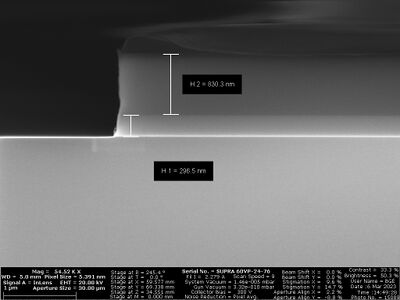
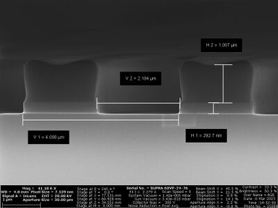
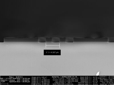
==Etch Profile SEM images== | ==Etch Profile SEM images== | ||
<gallery caption="Profile of etch for 'Slow Etch2' 12 min, 100mm wafer on 150mm carrier with double side | <gallery caption="Profile of etch for 'Slow Etch2' 12 min, 100mm wafer on 150mm carrier with double side polyimide tape (capton), Si3N4 from LPCVD" widths="300px done by bghe, DTU Nanolab" heights="300px" widths="400px" perrow="3"> | ||
File:C08507_01.jpg | File:C08507_01.jpg | ||
File:C08507_02.jpg | File:C08507_02.jpg | ||
| Line 102: | Line 102: | ||
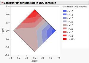
File:Contour Plot etch rates Si.jpg|Etch rate map of Si etch on 4" wafer (on 6" carrier) | File:Contour Plot etch rates Si.jpg|Etch rate map of Si etch on 4" wafer (on 6" carrier) | ||
</gallery> | </gallery> | ||
==Test section - do not use== | |||
{| class="wikitable" | |||
|+ Caption text | |||
|- | |||
! Header text !! Header text !! Header text | |||
|- | |||
| Example || Example || Example | |||
|- | |||
| Example || Example || Example | |||
|- | |||
| Example || Example || Example | |||
|} | |||
Revision as of 14:37, 28 June 2024
The slow etch
This work is done by Berit Herstrøm @DTU Nanolab, is nothing else is stated
The slow etch is designed to etch slow at low powers to etch thin films and to avoid overheating of samples mounted on a carrier with Capton/polyimide tape
| Parameter | Recipe name: Slow Etch | Recipe name: Slow Etch2 |
|---|---|---|
| Coil Power [W] | 350 | 200 |
| Platen Power [W] | 25 | 50 |
| Platen temperature [oC] | 20 | 20 |
| H2 flow [sccm] | 15 | 15 |
| CF4 flow [sccm] | 30 | 30 |
| Pressure [mTorr] | 3 | 10 |
| Typical results | Slow Etch | Slow Etch2 |
|---|---|---|
| Etch of SRN | ~43nm/min [measured 39-50 nm/min over a 6" wafer] | 23-25 nm/min [4" on carrier]] |
| Etch rate of Si3N4 | ~49 nm/min [4" on carrier] | 24-26 nm/min [4" on carrier] |
| Etch rate of SiO2 | ~42nm/min [41-43 nm/min over a 6" wafer] | 13.7-14.7 nm/min [4" on carrier] |
| Etch rate in Si | ñm/min | 11-13 nm/min (10% load, 4" wafer on 6" carrier) |
| Etch rate of Mir resist | ~nm/min | ~17 nm/min |
| Tested etch time without burning the resist | 3 min (6 min => resist burned) | 30 min |
| Profile [o] |
Etch Profile SEM images
- Profile of etch for 'Slow Etch2' 12 min, 100mm wafer on 150mm carrier with double side polyimide tape (capton), Si3N4 from LPCVD


Etch Uniformity maps
- Map of etch rate measurements for 'Slow Etch'
Etch rate map of SiO2 etch on 6" wafer
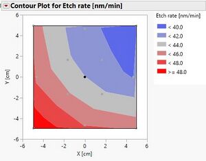
Etch rate map of SRN etch on 6" wafer


- Map of etch rate measurements for 'Slow Etch2'
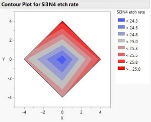
Etch rate map of Si3N4 etch on 4" wafer (on 6" carrier)
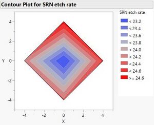
Etch rate map of SRN etch on 4" wafer (on 6" carrier)
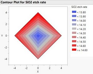
Etch rate map of SiO2 etch on 4" wafer (on 6" carrier)
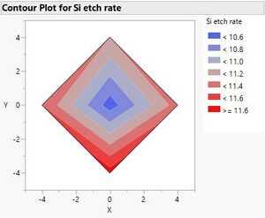
Etch rate map of Si etch on 4" wafer (on 6" carrier)


Test section - do not use
| Header text | Header text | Header text |
|---|---|---|
| Example | Example | Example |
| Example | Example | Example |
| Example | Example | Example |