Specific Process Knowledge/Characterization/XRD/Process Info: Difference between revisions
| (53 intermediate revisions by 2 users not shown) | |||
| Line 2: | Line 2: | ||
<i>This page is written by <b>Evgeniy Shkondin @DTU Nanolab</b> if nothing else is stated. <br> | <i>This page is written by <b>Evgeniy Shkondin @DTU Nanolab</b> if nothing else is stated. <br> | ||
All images and photos on this page | All images and photos on this page belongs to <b>DTU Nanolab</b>.</i> | ||
<span style="background:#FF2800">THIS PAGE IS UNDER CONSTRUCTION</span>[[image:Under_construction.png|200px]] | <span style="background:#FF2800">THIS PAGE IS UNDER CONSTRUCTION</span>[[image:Under_construction.png|200px]] | ||
= Process information = | |||
The following measurements types are just some of the options you have on the [http://labadviser.nanolab.dtu.dk/index.php?title=Specific_Process_Knowledge/Characterization/XRD/XRD_SmartLab Rigaku SmartLab] | The following measurements types are just some of the options you have on the [http://labadviser.nanolab.dtu.dk/index.php?title=Specific_Process_Knowledge/Characterization/XRD/XRD_SmartLab Rigaku SmartLab] | ||
==XRD for III-V materials== | |||
''(written by DTU Nanolab internal and DTU Fotonik staff)'' | |||
X-ray diffraction is a non-destructive technique which among many other things is able to measure the lattice mismatch of epitaxially grown layers. The applicable measurements are know as rocking-curves and reciprocal space maps and are described further below. Using these it is possible to find out the relative content of e.g. In in Ga<sub>x</sub>In<sub>1-x</sub>As grown on InP. Ga<sub>0.47</sub>In<sub>0.53</sub>As is lattice-matched to InP. Compounds containing three different materials are also called ternaries. | |||
For more complex compounds containing 4 elements, known as quaternaries, e.g. Ga<sub>x</sub>In<sub>1-x</sub>As<sub>y</sub>P<sub>1-y</sub>, it is possible to obtain both x and y by combining x-ray diffraction measurements and PL-measurements (see [[Specific Process Knowledge/Characterization/PL mapper|PL Mapper]]). | |||
== Slit selection (BB vs. PB)== | |||
<gallery caption="XPS recordings. 10 nm SiC deposited on Si wafer" widths="500px" heights="480px" perrow="2"> | |||
image:eves_BB_slit_selection_20230206.png|<b>C 1s</b> signal. | |||
image:eves_PB_slit_selection_20230206.png|<b>C 1s</b> signal. | |||
</gallery> | |||
= Bragg-Brentano= | |||
<gallery caption="XPS recordings. 10 nm SiC deposited on Si wafer" widths="700px" heights="480px" perrow="1"> | |||
image:eves_Bragg_Brentano_concept_20230206.png|<b>C 1s</b> signal. | |||
</gallery> | |||
= Parallel beam= | |||
==Types of scans in the reciprocal space== | ==Types of scans in the reciprocal space== | ||
| Line 15: | Line 33: | ||
</gallery> | </gallery> | ||
== | ==θ/2θ, 2θ/ω, and ω/2θ scans== | ||
<gallery caption="XPS recordings. 10 nm SiC deposited on Si wafer" widths="700px" heights="480px" perrow="1"> | |||
image:eves_XRD_drawing_series_T2T_20230206.png|<b>C 1s</b> signal. | |||
</gallery> | |||
<gallery caption="XPS recordings. 10 nm SiC deposited on Si wafer" widths="300px" heights="250px" perrow="3"> | <gallery caption="XPS recordings. 10 nm SiC deposited on Si wafer" widths="300px" heights="250px" perrow="3"> | ||
image:eves_theta2theta_scan_concept_20230131.png|<b>C 1s</b> signal. | image:eves_theta2theta_scan_concept_20230131.png|<b>C 1s</b> signal. | ||
| Line 32: | Line 47: | ||
==Rocking courve (ω scan)== | ==Rocking courve (ω scan)== | ||
<gallery caption="XPS recordings. 10 nm SiC deposited on Si wafer" widths=" | <gallery caption="XPS recordings. 10 nm SiC deposited on Si wafer" widths="700px" heights="480px" perrow="2"> | ||
image:eves_XRD_drawing_series_RC1_20230206.png|<b>C 1s</b> signal. | |||
image:eves_XRD_drawing_series_RC2_20230206.png|<b>C 1s</b> signal. | |||
</gallery> | |||
<gallery caption="XPS recordings. 10 nm SiC deposited on Si wafer" widths="500px" heights="300px" perrow="1"> | |||
image:eves_omega_scan_concept_20230131.png|<b>C 1s</b> signal. | image:eves_omega_scan_concept_20230131.png|<b>C 1s</b> signal. | ||
</gallery> | </gallery> | ||
| Line 41: | Line 61: | ||
[[File:RC.png|400px]] | [[File:RC.png|400px]] | ||
==2θ scan. Graizing Incident X-ray Diffraction(GiXRD)== | ==High Resolution XRD (HRXRD)== | ||
<gallery caption="XPS recordings. 10 nm SiC deposited on Si wafer" widths="700px" heights="480px" perrow="2"> | |||
image:eves_XRD_drawing_series_HRXRD1_20230206.png|<b>C 1s</b> signal. | |||
image:eves_XRD_drawing_series_HRXRD2_20230206.png|<b>C 1s</b> signal. | |||
</gallery> | |||
==2θ scan. Graizing Incident X-ray Diffraction (GiXRD)== | |||
<gallery caption="XPS recordings. 10 nm SiC deposited on Si wafer" widths="700px" heights="480px" perrow="1"> | |||
image:eves_XRD_drawing_series_GiXRD_20230206.png|<b>C 1s</b> signal. | |||
</gallery> | |||
For GIXRD you need a small incident slit (which is limited by the footprint on the wafer, so for a small incident angle and a small sample you will need even smaller incident slit size). However the receiving slits can be large / fully open as the PSA will anyway determine what diffraction angles are accepted into the detector. | |||
You can also use the 1D detector mode of the detector if you use an open PSA in the setup. This will speed up data collection. | |||
<gallery caption="XPS recordings. 10 nm SiC deposited on Si wafer" widths="500px" heights="300px" perrow="1"> | |||
image:eves_2theta_scan_concept_20230131.png|<b>C 1s</b> signal. | |||
</gallery> | |||
==RSM (Reciprocal Space Map) measurements== | |||
<gallery caption="XPS recordings. 10 nm SiC deposited on Si wafer" widths="1300px" heights="500px" perrow="1"> | |||
image:eves_RSM_scan_concept_20230131.png|<b>C 1s</b> signal. | |||
</gallery> | |||
==XRR== | |||
<gallery caption="XPS recordings. 10 nm SiC deposited on Si wafer" widths="700px" heights="150px" perrow="2"> | |||
image:eves_XRD_drawing_series_XRR1_20230206.png|<b>C 1s</b> signal. | |||
image:eves_XRD_drawing_series_XRR2_20230206.png|<b>C 1s</b> signal. | |||
</gallery> | |||
[[/The Principles of X-ray Reflectivity Analysis|The principles of X-ray reflectivity analysis (XRR)]] | |||
With X-Ray Reflectivity measurements, it is possible to obtain information on thickness, density, and both surface and interface roughness on thin films. The technique does not depend on crystal structure and can be used on both amorphous, poly-, and single-crystalline materials. | |||
For film thickness measurement, films up to around 100 nm can be measured. You are welcome to try it on thicker films, but please confirm the measurement the first time by use of other equipment. XRR is a special case of a Theta/2Theta measurement. | |||
Rigaku gives a good explanation of the principles behind the XRR in [https://labmanager.dtu.dk/view_binary.php?fileId=4937|this paper] - requires login. | |||
==Pole | It's a good idea to use a very small incident slit as suggested by default by the Rigaku software (0.05 mm) and also use very small receiving slits to reduce background noise, e.g., RS1 = IS and RS2 sligthly larger. | ||
==In-Plane Measurements 2θχ or 2θχ/φ scans == | |||
==Residual Stress== | |||
==Texture (Pole figures)== | |||
Pole figures can be used to determine the orientation of a crystal. For polycrystalline materials, it is possible to determine if there is a preferred direction of the crystal grains. In a pole figure, a measurement of a predefined peek for the material is measured in the half sphere above the sample. This will result in a map of intensities in relation to the angles from the surface normal and along sample rotation. For instance if you have a single crystalline sample with a [0 0 1] surface and measure on the [1 1 1] lattice plane, you should find 4 peaks spaced 90° in beta and at 35.26° in alpha. | Pole figures can be used to determine the orientation of a crystal. For polycrystalline materials, it is possible to determine if there is a preferred direction of the crystal grains. In a pole figure, a measurement of a predefined peek for the material is measured in the half sphere above the sample. This will result in a map of intensities in relation to the angles from the surface normal and along sample rotation. For instance if you have a single crystalline sample with a [0 0 1] surface and measure on the [1 1 1] lattice plane, you should find 4 peaks spaced 90° in beta and at 35.26° in alpha. | ||
| Line 127: | Line 194: | ||
[[File:PoleFigureAngles.png|400px]][[File:Overlay.png|400px]] | [[File:PoleFigureAngles.png|400px]][[File:Overlay.png|400px]] | ||
Rigaku describes Pole figures [ | |||
Rigaku describes Pole figures [https://labmanager.dtu.dk/view_binary.php?fileId=4939 in this paper] - requires login | |||
Latest revision as of 11:29, 21 December 2023
Feedback to this page: click here
This page is written by Evgeniy Shkondin @DTU Nanolab if nothing else is stated.
All images and photos on this page belongs to DTU Nanolab.
THIS PAGE IS UNDER CONSTRUCTION
Process information
The following measurements types are just some of the options you have on the Rigaku SmartLab
XRD for III-V materials
(written by DTU Nanolab internal and DTU Fotonik staff)
X-ray diffraction is a non-destructive technique which among many other things is able to measure the lattice mismatch of epitaxially grown layers. The applicable measurements are know as rocking-curves and reciprocal space maps and are described further below. Using these it is possible to find out the relative content of e.g. In in GaxIn1-xAs grown on InP. Ga0.47In0.53As is lattice-matched to InP. Compounds containing three different materials are also called ternaries. For more complex compounds containing 4 elements, known as quaternaries, e.g. GaxIn1-xAsyP1-y, it is possible to obtain both x and y by combining x-ray diffraction measurements and PL-measurements (see PL Mapper).
Slit selection (BB vs. PB)
- XPS recordings. 10 nm SiC deposited on Si wafer
-
C 1s signal.
-
C 1s signal.
Bragg-Brentano
- XPS recordings. 10 nm SiC deposited on Si wafer
-
C 1s signal.
Parallel beam
Types of scans in the reciprocal space
- XPS recordings. 10 nm SiC deposited on Si wafer
-
C 1s signal.
θ/2θ, 2θ/ω, and ω/2θ scans
- XPS recordings. 10 nm SiC deposited on Si wafer
-
C 1s signal.
- XPS recordings. 10 nm SiC deposited on Si wafer
-
C 1s signal.
-
C 1s signal.
-
C 1s signal.
A theta-2theta scan can be used for identifying peaks and hence lattice constants and possible crystal orientations. It will also be possible to say something about the materials of the crystal, but it is not suitable for identification of composition. If a multilayers structure is present a simulation of the structure and comparison to the measurement can help identify layer thicknesses, atomic ratios, and interface roughnesses.
Rocking courve (ω scan)
- XPS recordings. 10 nm SiC deposited on Si wafer
-
C 1s signal.
-
C 1s signal.
- XPS recordings. 10 nm SiC deposited on Si wafer
-
C 1s signal.
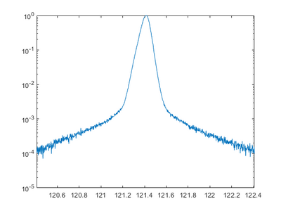
A rocking curve is measured by fixing the 2Theta angle and changing the incident angle omega, which is the same as rocking the sample in the setup. This can be used to determine the preferred orientation and the degree of orientation of the measured material. For a perfect crystal and rocking curve will show a single sharp peak, if the layers are not perfect crystalline the diffraction peak will broaden. If an epitaxial layer is grown on a preface substrate, and the sample alignment is done to the substrate peak, a shift in omega will indicate a tilt in the crystal planes. A broadening could mean a dislocations, mosaicity, or curvature of the sample.
High Resolution XRD (HRXRD)
- XPS recordings. 10 nm SiC deposited on Si wafer
-
C 1s signal.
-
C 1s signal.
2θ scan. Graizing Incident X-ray Diffraction (GiXRD)
- XPS recordings. 10 nm SiC deposited on Si wafer
-
C 1s signal.
For GIXRD you need a small incident slit (which is limited by the footprint on the wafer, so for a small incident angle and a small sample you will need even smaller incident slit size). However the receiving slits can be large / fully open as the PSA will anyway determine what diffraction angles are accepted into the detector.
You can also use the 1D detector mode of the detector if you use an open PSA in the setup. This will speed up data collection.
- XPS recordings. 10 nm SiC deposited on Si wafer
-
C 1s signal.
RSM (Reciprocal Space Map) measurements
- XPS recordings. 10 nm SiC deposited on Si wafer
-
C 1s signal.
XRR
- XPS recordings. 10 nm SiC deposited on Si wafer
-
C 1s signal.
-
C 1s signal.
The principles of X-ray reflectivity analysis (XRR)
With X-Ray Reflectivity measurements, it is possible to obtain information on thickness, density, and both surface and interface roughness on thin films. The technique does not depend on crystal structure and can be used on both amorphous, poly-, and single-crystalline materials.
For film thickness measurement, films up to around 100 nm can be measured. You are welcome to try it on thicker films, but please confirm the measurement the first time by use of other equipment. XRR is a special case of a Theta/2Theta measurement.
Rigaku gives a good explanation of the principles behind the XRR in paper - requires login.
It's a good idea to use a very small incident slit as suggested by default by the Rigaku software (0.05 mm) and also use very small receiving slits to reduce background noise, e.g., RS1 = IS and RS2 sligthly larger.
In-Plane Measurements 2θχ or 2θχ/φ scans
Residual Stress
Texture (Pole figures)
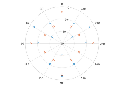
Pole figures can be used to determine the orientation of a crystal. For polycrystalline materials, it is possible to determine if there is a preferred direction of the crystal grains. In a pole figure, a measurement of a predefined peek for the material is measured in the half sphere above the sample. This will result in a map of intensities in relation to the angles from the surface normal and along sample rotation. For instance if you have a single crystalline sample with a [0 0 1] surface and measure on the [1 1 1] lattice plane, you should find 4 peaks spaced 90° in beta and at 35.26° in alpha.
Peak angles can be calculated by simple vector calculations; however, We have made a small MATLAB script calculating them for you. To use the script open MATLAB and call the program with two vectors as input. First vector should be your surface orientation, second input the plane you measure on. For a [1 1 1] substrate surface and a [3 1 1] plane and a [0 0 1] substrate surface and a [1 3 3] plane, where the measurement planes are dependent on the 2theta angle, the command looks like this:
| PoleFigureAngles([1 1 1; 0 0 1],[3 1 1; 1 3 3]) |
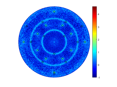
It is also possible to give a path for a file exported from 3D Explore with contour data from a measurement, and a rotational correction for the data:
| PoleFigureAngles([1 1 1; 0 0 1],[3 1 1; 1 3 3],'\Au_thin_inplanepole_WF1_m2.txt',30.9) |
Which will give the following table and pictures, without a file input only the table and the first graph will be given:
| Alpha | Beta | Alpha | Beta |
|---|---|---|---|
| 10.02 | 60.00 | 13.26 | 0.00 |
| 10.02 | 300.00 | 13.26 | 270.00 |
| 10.02 | 180.00 | 13.26 | 90.00 |
| 31.48 | 30.00 | 13.26 | 180.00 |
| 31.48 | 330.00 | 43.49 | 333.43 |
| 31.48 | 90.00 | 43.49 | 296.57 |
| 31.48 | 270.00 | 43.49 | 26.57 |
| 31.48 | 150.00 | 43.49 | 243.43 |
| 31.48 | 210.00 | 43.49 | 63.43 |
| 60.50 | 60.00 | 43.49 | 206.57 |
| 60.50 | 300.00 | 43.49 | 116.57 |
| 60.50 | 180.00 | 43.49 | 153.43 |
Rigaku describes Pole figures in this paper - requires login


