Specific Process Knowledge/Etch/DRIE-Pegasus/Pegasus-4/SiO2 Etch/Cr mask: Difference between revisions
No edit summary |
No edit summary |
||
| Line 2: | Line 2: | ||
{{CC-bghe2}} | {{CC-bghe2}} | ||
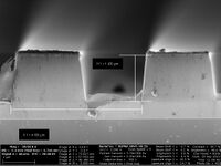
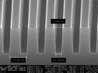
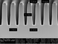
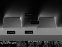
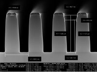
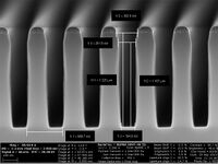
<gallery caption="EM tests with Cr mask on full wafer 6 min etch" perrow=" | <gallery caption="EM tests with Cr mask on full wafer 6 min etch" perrow="6" widths="200px" heights="150px"> | ||
File:C09721_center_05.jpg | File:C09721_center_05.jpg | ||
File:C09721_center_07.jpg | File:C09721_center_07.jpg | ||
| Line 9: | Line 9: | ||
File:C09721_center_21.jpg | File:C09721_center_21.jpg | ||
File:C09721_center_22.jpg | File:C09721_center_22.jpg | ||
</gallery> | |||
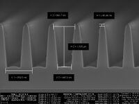
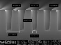
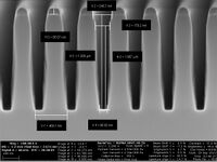
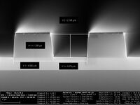
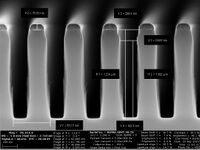
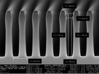
<gallery caption="EM tests with Cr mask on wafer piece on Si carrier 6 min etch" perrow="6" widths="200px" heights="150px"> | |||
File:C10022_03__02.jpg | |||
File:C10022_03__04.jpg | |||
File:C10022_03__06.jpg | |||
File:C10022_03__08.jpg | |||
File:C10022_03__10.jpg | |||
File:C10022_03__12.jpg | |||
</gallery> | |||
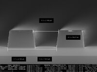
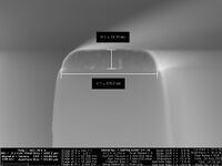
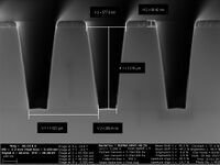
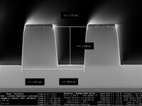
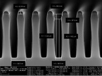
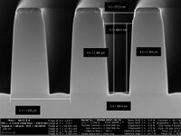
<gallery caption="EM tests with Cr mask on full wafer 6 min etch" perrow="6" widths="200px" heights="150px"> | |||
File:C10025_03__01.jpg | |||
File:C10025_03__03.jpg | |||
File:C10025_03__05.jpg | |||
File:C10025_03__07.jpg | |||
File:C10025_03__09.jpg | |||
File:C10025_03__11.jpg | |||
</gallery> | |||
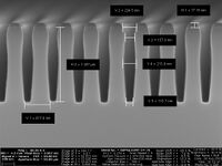
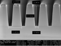
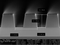
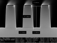
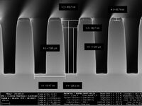
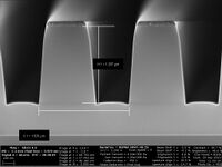
<gallery caption="EM tests with Cr mask on full wafer 6 min etch" perrow="6" widths="200px" heights="150px"> | |||
File:C10026_03__01.jpg | |||
File:C10026_03__03.jpg | |||
File:C10026_03__05.jpg | |||
File:C10026_03__07.jpg | |||
File:C10026_03__09.jpg | |||
File:C10026_03__10.jpg | |||
</gallery> | </gallery> | ||
Revision as of 13:52, 21 September 2023
Feedback to this page: click here
Unless otherwise stated, all content in this section was done by Berit Herstrøm, DTU Nanolab
- EM tests with Cr mask on full wafer 6 min etch
-
-
-
-
-
-


- EM tests with Cr mask on wafer piece on Si carrier 6 min etch
-
-
-
-
-
-


- EM tests with Cr mask on full wafer 6 min etch
-
-
-
-
-
-


- EM tests with Cr mask on full wafer 6 min etch
-
-
-
-
-
-