Specific Process Knowledge/Thin film deposition/PECVD/Doping: Difference between revisions
| (13 intermediate revisions by 2 users not shown) | |||
| Line 1: | Line 1: | ||
'''Feedback to this page''': '''[mailto:labadviser@ | '''Feedback to this page''': '''[mailto:labadviser@nanolab.dtu.dk?Subject=Feed%20back%20from%20page%20http://labadviser.nanolab.dtu.dk/index.php/Specific_Process_Knowledge/Thin_film_deposition/PECVD/Doping click here]''' | ||
=<span style="color:#FF0000">This work has been done on PECVD2. PECVD2 has been decomissioned but we keep this information because we expect PECVD3 and PECVD4 to behave similar</span>= | |||
==Boron-doping by use of BSG glass deposited in PECVD2== | |||
''Results from Joachim Dahl Thomsen, Nanotech, 2014'' | |||
= | ===Recipe=== | ||
{| border="1" cellspacing="0" cellpadding="7" width="800" style="text-align:center;" | |||
|- | |||
|Recipe name | |||
|SiH<sub>4</sub> flow [sccm] | |||
|N<sub>2</sub>O flow [sccm] | |||
|N2 flow [sccm] | |||
|B<sub>2</sub>H<sub>6</sub> flow [sccm] | |||
|PH<sub>3</sub> flow [sccm] | |||
|Pressure [mTorr] | |||
|Power [W] | |||
|Description | |||
|- | |||
|1PBSG | |||
|17 | |||
|1600 | |||
|0 | |||
|120, 130, 140, 160, 240 | |||
|0 | |||
|400 | |||
|380 | |||
|BSG glass for driving in boron in Silicon | |||
|} | |||
==Boron-doping by use of BSG glass deposited in | 5 tests were made where only the B<sub>2</sub>H<sub>6</sub> flow was changed for each deposition (120sccm,130sccm,140sccm,160sccm,240sccm). All deposition times were 2 min, resulting in 440 nm Oxide. | ||
The wafers were annealed in Anneal Oxide Furnace (C1) at 1000°C for 85 min to drive in the boron and the oxide was subsequently etched in BHF. | |||
The wafers were then analyzed by SIMS and the results are shown in the figure below: | |||
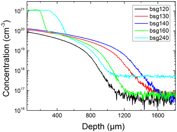
[[image:SIMS2.png|627x424px|left|thumb|Boron concentration measured by SIMS. Results from Joachim Dahl Thomsen, Nanotech, 2014.]] | |||
<br clear="all" /> | |||
==Boron-doping by use of BSG glass deposited in PECVD2== | |||
''Results from Trine Holm Christensen, Space, Feb. 2015'' | |||
===Recipe=== | ===Recipe=== | ||
{| border="1" cellspacing="0" cellpadding="7" | {| border="1" cellspacing="0" cellpadding="7" width="800" style="text-align:center;" | ||
|- | |- | ||
|Recipe name | |Recipe name | ||
| | |SiH<sub>4</sub> flow [sccm] | ||
|N<sub>2</sub>O flow [sccm] | |N<sub>2</sub>O flow [sccm] | ||
|N2 flow [sccm] | |N2 flow [sccm] | ||
| | |B<sub>2</sub>H<sub>6</sub> flow [sccm] | ||
| | |PH<sub>3</sub> flow [sccm] | ||
|Pressure [mTorr] | |Pressure [mTorr] | ||
|Power [W] | |Power [W] | ||
| Line 25: | Line 62: | ||
|1600 | |1600 | ||
|0 | |0 | ||
|120, 130, 140 | |120, 130, 140 | ||
|0 | |0 | ||
|400 | |400 | ||
|380 | |380 | ||
| | |BSG glass for driving in boron in Silicon | ||
|} | |} | ||
3 tests were made where only the B<sub>2</sub>H<sub>6</sub> flow was changed for each deposition (120sccm,130sccm,140sccm,160sccm,240sccm). All deposition times were 2 min, resulting in approximately 400nm Oxide. | |||
The wafers were going through several annealing and oxidation step: | |||
[[image: | '''The total thermal budget for the wafers:''' | ||
'''Anneal in Furnace (C1):''' ANN1000, 30 min in N<sub>2</sub>, strip of oxide in a 25 min BHF etch. | |||
'''Wet oxidation in Furnace (C1):''' WET1050, 30 min, no further anneal | |||
'''Anneal in Furnace (C1):''' ANN950, 60 min in N<sub>2</sub> | |||
The wafers were then analyzed by SIMS and the results are shown in the figure below: | |||
[[image:PECVD_Boron_doping_profiles.jpg|627x424px|left|thumb|Boron concentration measured by SIMS. Results from Trine Holm Christensen, Space, Feb. 2015.]] | |||
<br clear="all" /> | |||
Measured peak concentrations and sheet resistances: | |||
<br> | |||
{| border="1" cellspacing="0" cellpadding="7" with="50" style="text-align:center;" | |||
|- | |||
|Wafer | |||
|Peak Concentration | |||
[atoms/cm<sup>3</sup>] | |||
|Sheet Resistance | |||
[Ω/sq] | |||
|- | |||
|BSG120 | |||
|1.75*10<sup>19</sup> | |||
|56.4 | |||
|- | |||
|BSG130 | |||
|2.44*10<sup>19</sup> | |||
|36.2 | |||
|- | |||
|BSG140 | |||
|2.36*10<sup>19</sup> | |||
|40.3 | |||
|- | |||
|} | |||
<br clear="all" /> | <br clear="all" /> | ||
Latest revision as of 14:08, 7 August 2023
Feedback to this page: click here
This work has been done on PECVD2. PECVD2 has been decomissioned but we keep this information because we expect PECVD3 and PECVD4 to behave similar
Boron-doping by use of BSG glass deposited in PECVD2
Results from Joachim Dahl Thomsen, Nanotech, 2014
Recipe
| Recipe name | SiH4 flow [sccm] | N2O flow [sccm] | N2 flow [sccm] | B2H6 flow [sccm] | PH3 flow [sccm] | Pressure [mTorr] | Power [W] | Description |
| 1PBSG | 17 | 1600 | 0 | 120, 130, 140, 160, 240 | 0 | 400 | 380 | BSG glass for driving in boron in Silicon |
5 tests were made where only the B2H6 flow was changed for each deposition (120sccm,130sccm,140sccm,160sccm,240sccm). All deposition times were 2 min, resulting in 440 nm Oxide. The wafers were annealed in Anneal Oxide Furnace (C1) at 1000°C for 85 min to drive in the boron and the oxide was subsequently etched in BHF.
The wafers were then analyzed by SIMS and the results are shown in the figure below:

Boron-doping by use of BSG glass deposited in PECVD2
Results from Trine Holm Christensen, Space, Feb. 2015
Recipe
| Recipe name | SiH4 flow [sccm] | N2O flow [sccm] | N2 flow [sccm] | B2H6 flow [sccm] | PH3 flow [sccm] | Pressure [mTorr] | Power [W] | Description |
| 1PBSG | 17 | 1600 | 0 | 120, 130, 140 | 0 | 400 | 380 | BSG glass for driving in boron in Silicon |
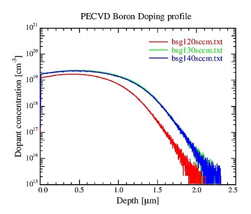
3 tests were made where only the B2H6 flow was changed for each deposition (120sccm,130sccm,140sccm,160sccm,240sccm). All deposition times were 2 min, resulting in approximately 400nm Oxide.
The wafers were going through several annealing and oxidation step:
The total thermal budget for the wafers:
Anneal in Furnace (C1): ANN1000, 30 min in N2, strip of oxide in a 25 min BHF etch.
Wet oxidation in Furnace (C1): WET1050, 30 min, no further anneal
Anneal in Furnace (C1): ANN950, 60 min in N2
The wafers were then analyzed by SIMS and the results are shown in the figure below:

Measured peak concentrations and sheet resistances:
| Wafer | Peak Concentration
[atoms/cm3] |
Sheet Resistance
[Ω/sq] |
| BSG120 | 1.75*1019 | 56.4 |
| BSG130 | 2.44*1019 | 36.2 |
| BSG140 | 2.36*1019 | 40.3 |
