Specific Process Knowledge/Etch/Etching of Silicon Oxide/SiO2 etch using ASE/ICP recipe for SiO2: Difference between revisions
Jump to navigation
Jump to search
| (22 intermediate revisions by the same user not shown) | |||
| Line 1: | Line 1: | ||
''' ''Unless otherwise stated, all content in this section was done by Maria Farinha@DTU Nanolab, May 2023'' ''' | |||
This recipe was taken from the ICP Metal etch, with a slight difference in the platen temperature. | This recipe was taken from the ICP Metal etch, with a slight difference in the platen temperature. | ||
{| border="1" cellspacing="2" cellpadding="2" | {| border="1" cellspacing="2" cellpadding="2" | ||
| Line 27: | Line 28: | ||
|} | |} | ||
====Results | ====Results with a ''non-patterned wafer''==== | ||
{| border="2" cellspacing="2" cellpadding="3" | |||
|-style="background:DarkGray; color:White" | |||
!Recipe | |||
!Recipe: SIO2_ICP | |||
!SIO2_ICP on stoic Nit | |||
!SIO2_ICP on low-stress Nit | |||
|- | |||
|Etch rate | |||
|121 nm/min | |||
(18.07.2023 mfarin @ DTU nanolab) | |||
|194 nm/min | |||
(24.05.2023 mfarin @ DTU nanolab) | |||
|190 nm/min | |||
(24.05.2023 mfarin @ DTU nanolab) | |||
|- | |||
|} | |||
====Results with a ''patterned wafer'' ==== | |||
{| border="2" cellspacing="2" cellpadding="3" | {| border="2" cellspacing="2" cellpadding="3" | ||
| Line 40: | Line 62: | ||
|155 nm/min in the center, 125nm/min in the edges | |155 nm/min in the center, 125nm/min in the edges | ||
(03052023 mfarin @ DTU nanolab) | (03052023 mfarin @ DTU nanolab) | ||
| | | | ||
| | | | ||
| | | | ||
|- | |- | ||
| Line 73: | Line 95: | ||
|- | |- | ||
|} | |} | ||
*More tests will be done regarding silicon and silicon nitride, since this recipe can be used for overetch. | |||
<br clear="all" /> | <br clear="all" /> | ||
Latest revision as of 15:25, 18 July 2023
Unless otherwise stated, all content in this section was done by Maria Farinha@DTU Nanolab, May 2023
This recipe was taken from the ICP Metal etch, with a slight difference in the platen temperature.
| Parameter | Recipe name: SiO2_ICP |
|---|---|
| Coil Power [W] | 1000 |
| Platen Power [W] | 200 |
| Platen temperature [oC] | 20 |
| C4F8 flow [sccm] | 10 |
| H2 flow [sccm] | 28 |
| Pressure [mTorr] | 2.5 |
Results with a non-patterned wafer
| Recipe | Recipe: SIO2_ICP | SIO2_ICP on stoic Nit | SIO2_ICP on low-stress Nit |
|---|---|---|---|
| Etch rate | 121 nm/min
(18.07.2023 mfarin @ DTU nanolab) |
194 nm/min
(24.05.2023 mfarin @ DTU nanolab) |
190 nm/min
(24.05.2023 mfarin @ DTU nanolab) |
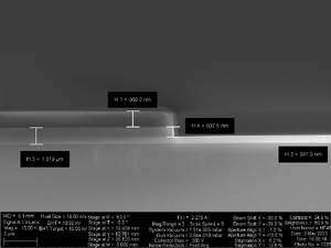
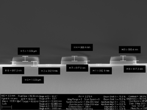
Results with a patterned wafer
- More tests will be done regarding silicon and silicon nitride, since this recipe can be used for overetch.

