Specific Process Knowledge/Thin film deposition/ALD Picosun R200/ZnO deposition using ALD: Difference between revisions
No edit summary |
No edit summary |
||
| (32 intermediate revisions by 4 users not shown) | |||
| Line 1: | Line 1: | ||
'''Feedback to this page''': '''[mailto:labadviser@nanolab.dtu.dk?Subject=Feed%20back%20from%20page%20http://labadviser.nanolab.dtu.dk/index.php/Specific_Process_Knowledge/Thin_film_deposition/ALD_Picosun_R200/ZnO_deposition_using_ALD click here]''' | |||
''This page is written by DTU Nanolab internal'' | |||
<b>Recipe: | <br clear="all" /> | ||
====''Obsolete - ZnO should now be deposited in ALD2''==== | |||
<br clear="all" /> | |||
Deposition of ZnO is a standard, well-explored ALD process. | |||
Previously (before 2018), DEZ had its independent inlet (A1), which shared the same N2 line with the TiCl4 precursor (A2). The DEZ precursor bottle was placed in a cabinet behind the instrument in the service area, and a long pipe led the precursor to the ALD chamber. This option has been abandoned due to safety reasons. This line was very difficult to purge in case of service. The results that were obtained with the old hardware configuration now remain [[Specific_Process_Knowledge/Thin_film_deposition/ALD_Picosun_R200/ZnO deposition using ALD/Obsolete|obsolete]]. | |||
Nowadays, if the user wants to deposit ZnO, in ALD-1 the diethyl zinc (DEZ) has to be mounted in the A-line. If TiCl4 is currently present it has to be exchanged with DEZ. This is a time-consuming job, that needs to be ordered and prepared in advance. | |||
=ZnO ALD deposition using DEZ and H<sub>2</sub>O= | |||
ZnO can be deposited in the range between 100 <sup>o</sup>C to 225 <sup>o</sup>C. It is not recommended to increase the temperature above 225<sup>o</sup>C, as the uniformity suffers due to the precursor decomposition. The maximum temperature can be 250<sup>o</sup>C, here however the film crystal quality, crystallinity, roughness, etc. sufficiently differ from the films prepared in a lower temperature range. | |||
All results shown on this page have been obtained using the present (from 2018) configuration. | |||
Deposition and characterization has been performed in <b>2021 by Evgeniy Shkondin, DTU Nanolab</b> | |||
=ZnO recipes= | |||
==<b>Recipe: ZnO</b>== | |||
<b>Maximum deposition thickness: 100 nm</b> | <b>Maximum deposition thickness: 100 nm</b> | ||
<b>Temperature: 100 <sup>o</sup>C - | <b>Temperature: 100 <sup>o</sup>C - 250 <sup>o</sup>C</b> | ||
{| border="2" cellspacing="2" cellpadding="5" align="none" | {| border="2" cellspacing="2" cellpadding="5" align="none" | ||
|- | |- | ||
| | | | ||
! | !DEZ* | ||
!H<sub>2</sub>O | !H<sub>2</sub>O | ||
|- | |- | ||
| Line 26: | Line 45: | ||
|- | |- | ||
!Purge time | !Purge time | ||
| | |5.0 s | ||
| | |5.0 s | ||
|- | |- | ||
|} | |} | ||
This is | This is a standard recipe of ZnO. It is suitable for coating the flat samples and structures with an aspect ratio of around up to 1:10. | ||
== | ==<b>Recipe: ZnOT</b>== | ||
<b>Maximum deposition thickness: 100 nm</b> | |||
<b>Temperature: 100 <sup>o</sup>C - 250 <sup>o</sup>C</b> | |||
{| border="2" cellspacing="2" cellpadding="5" align="none" | |||
|- | |||
| | |||
!DEZ<sup>*</sup> | |||
!DEZ | |||
!H<sub>2</sub>O | |||
!H<sub>2</sub>O | |||
|- | |||
!Nitrogen flow | |||
|150 sccm | |||
|150 sccm | |||
|200 sccm | |||
|200 sccm | |||
|- | |||
!Pulse time | |||
|0.1 s | |||
|0.1 s | |||
|0.1 s | |||
|0.1 s | |||
|- | |||
!Purge time | |||
|0.5 s | |||
|20.0 s | |||
|0.5 s | |||
|20.0 s | |||
|- | |||
|} | |||
<br clear="all" /> | |||
This is a more complicated recipe that allows coating the sample with very high aspect ratio profiles. One SEM example is shown on one of the images below. The recipe is good for deposition on very high aspect ratio structures (with aspect ratio more than 1:20) such as deep trenches, pillars, pores etc. <b>ZnOT</b> recipe can also be used for deposition on polymers at low temperatures (80-120 <sup>o</sup>C). | |||
<br clear="all" /> | <br clear="all" /> | ||
<strong>DEZ</strong> is diethylzinc Zn(CH<sub>2</sub>CH<sub>3</sub>)<sub>2</sub> or ZnEt<sub>2</sub> | |||
<br clear="all" /> | <br clear="all" /> | ||
= | =Deposition characteristics= | ||
The deposition rate for ZnO depends on the temperature, see the ALD-window graph below. The uniformity, thickness, refractive index has been obtained using Ellipsometer VASE. | |||
==Deposition rate== | |||
In the graphs below the ZnO thickness vs. number of cycles for deposition temperatures between 100 <sup>o</sup>C and 250 <sup>o</sup>C presented. Results have been obtained for <100> 100 mm Si wafers with native oxide, based on [[Specific_Process_Knowledge/Characterization/Optical_characterization#Ellipsometer|ellipsometry]] study. The optical model used in fitting is based on Tauc-Lorentz and two Lorentz oscillators. | |||
|- | |||
<gallery caption="" widths="400px" heights="400px" perrow="2"> | |||
image:eves_dep_rate_ZnO_100C_ALD1_20220223.png|Deposition rate of ZnO at 100 <sup>o</sup>C. Substrate: Silicon 4" wafer with native oxide. <br> <math> Thickness (nm) = 0.1483 \cdot N + 0.63 </math> | |||
image:eves_dep_rate_ZnO_150C_ALD1_20220223.png|Deposition rate of ZnO at 150 <sup>o</sup>C. Substrate: Silicon 4" wafer with native oxide. <br> <math> Thickness (nm) = 0.1954 \cdot N - 2.73 </math> | |||
image:eves_dep_rate_ZnO_200C_ALD1_20220223.png|Deposition rate of ZnO at 200 <sup>o</sup>C. Substrate: Silicon 4" wafer with native oxide. <br> <math> Thickness (nm) = 0.1842 \cdot N - 3.80 </math> | |||
image:eves_dep_rate_ZnO_250C_ALD1_20220223.png|Deposition rate of ZnO at 250 <sup>o</sup>C. Substrate: Silicon 4" wafer with native oxide. <br> <math> Thickness (nm) = 0.1326 \cdot N + 1.13 </math> | |||
image:eves_ALD_window_ZnO_ALD1_20220223.png|ALD window of ZnO | |||
</gallery> | |||
<br clear="all" /> | |||
==Uniformity across 100 mm wafer== | |||
Recipe "ZnO" Samples: 100mm ssp-Si | |||
| | Results have been obtained for <100> 100 mm Si wafers with native oxide, based on [[Specific_Process_Knowledge/Characterization/Optical_characterization#Ellipsometer|ellipsometry]] study. | ||
| | {| border="2" cellspacing="0" cellpadding="9" | ||
| | !colspan="1" border="none" style="background:silver; color:black;" align="center"|Temperature (°C) / Number of cycles | ||
| | |style="background:silver; color:black"|<b>Deposition rate (nm/s)</b> | ||
| | |style="background:silver; color:black"|<b>Average thickness (nm)</b> | ||
| | |style="background:silver; color:black"|<b>Standard deviation</b> | ||
| | |style="background:silver; color:black"|<b>Uniformity (%)</b> | ||
| | |||
|- | |- | ||
| | !style="background:silver; color:black;" align="center" |100°C / 500cycles | ||
|style="background:WhiteSmoke; color:black" align="center"|<b><span style="color: red">0.1483</span></b> | |||
| | |style="background:WhiteSmoke; color:black" align="center"|75.67 | ||
| | |||
| | |style="background:WhiteSmoke; color:black" align="center"|1.49 | ||
|1. | |||
| | |style="background:WhiteSmoke; color:black" align="center"|3.26 | ||
| | |||
|- | |- | ||
| | !style="background:silver; color:black;" align="center" |150°C / 500cycles | ||
|style="background:WhiteSmoke; color:black" align="center"|<b><span style="color: red">0.1954</span></b> | |||
|style="background:WhiteSmoke; color:black" align="center"|95.32 | |||
|style="background:WhiteSmoke; color:black" align="center"|1.32 | |||
| | |||
|style="background:WhiteSmoke; color:black" align="center"|2.44 | |||
|- | |- | ||
! | !style="background:silver; color:black;" align="center" |200°C / 500cycles | ||
| | |||
| | |style="background:WhiteSmoke; color:black" align="center"|<b><span style="color: red">0.1842</span></b> | ||
| | |||
| | |style="background:WhiteSmoke; color:black" align="center"|87.97 | ||
| | |||
|style="background:WhiteSmoke; color:black" align="center"|0.31 | |||
| | |style="background:WhiteSmoke; color:black" align="center"|0.63 | ||
| | |||
|- | |- | ||
| | !style="background:silver; color:black;" align="center" |225°C / 500cycles | ||
| | |style="background:WhiteSmoke; color:black" align="center"|<b><span style="color: red">0.1622</span></b> | ||
|0. | |||
| | |style="background:WhiteSmoke; color:black" align="center"|81.09 | ||
| | |||
| | |style="background:WhiteSmoke; color:black" align="center"|0.45 | ||
|0. | |||
|style="background:WhiteSmoke; color:black" align="center"|1.07 | |||
|- | |- | ||
| | !style="background:silver; color:black;" align="center" |250°C / 500cycles | ||
|style="background:WhiteSmoke; color:black" align="center"|<b><span style="color: red">0.1326</span></b> | |||
|style="background:WhiteSmoke; color:black" align="center"|67.92 | |||
| | |||
| | |style="background:WhiteSmoke; color:black" align="center"|1.71 | ||
|1. | |||
| | |style="background:WhiteSmoke; color:black" align="center"|3.82 | ||
| | |||
|- | |- | ||
| | |} | ||
<br> | |||
<!-- --> | |||
| | <gallery caption="" widths="400px" heights="400px" perrow="3"> | ||
|150 | image:eves_SE_uniformity_ZnO_100C_ALD1_20220223.png|Uniformity across 100mm wafer. Deposition at 100°C | ||
| | image:eves_SE_uniformity_ZnO_150C_ALD1_20220223.png|Uniformity across 100mm wafer. Deposition at 150°C | ||
| | image:eves_SE_uniformity_ZnO_200C_ALD1_20220223.png|Uniformity across 100mm wafer. Deposition at 200°C | ||
| | image:eves_SE_uniformity_ZnO_225C_ALD1_20220223.png|Uniformity across 100mm wafer. Deposition at 225°C | ||
image:eves_SE_uniformity_ZnO_250C_ALD1_20220223.png|Uniformity across 100mm wafer. Deposition at 250°C | |||
</gallery> | |||
=Optical functions= | |||
| | Results have been obtained for <100> 100 mm Si wafers with native oxide, based on [[Specific_Process_Knowledge/Characterization/Optical_characterization#Ellipsometer|ellipsometry]] study. | ||
<gallery caption="" widths="400px" heights="400px" perrow="2"> | |||
image:eves_ref_index_ZnO_ALD1_20220223.png|Refractive index. | |||
| | image:eves_abs_coeff_ZnO_ALD1_20220223.png|Absorption coefficient. | ||
</gallery> | |||
| | |||
=SEM images= | |||
| | Images obtained using [[Specific Process Knowledge/Characterization/SEM: Scanning Electron Microscopy|SEM inspection]]. | ||
< | <gallery caption="" widths="400px" heights="400px" perrow="3"> | ||
<b> | image:eves_SEM_ZnO_500cycles_100C_ALD1_20220223_convert.png|SEM image of flat surface of ZnO. Deposition at 100°C | ||
image:eves_SEM_ZnO_500cycles_150C_ALD1_20220223_convert.png|SEM image of flat surface of ZnO. Deposition at 150°C | |||
< | image:eves_SEM_ZnO_500cycles_200C_ALD1_20220223_convert.png|SEM image of flat surface of ZnO. Deposition at 200°C | ||
image:eves_SEM_ZnO_500cycles_225C_ALD1_20220223_convert.png|SEM image of flat surface of ZnO. Deposition at 225°C | |||
image:eves_SEM_ZnO_500cycles_250C_ALD1_20220223_convert.png|SEM image of flat surface of ZnO. Deposition at 250°C | |||
image:eves_SEM_ZnO_HARS_ALD1_20220223_convert.png|ZnO deposition example on high aspect ratio structures. "<b>ZnOT</b>" recipe was used. | |||
</gallery> | |||
= | =ZnO XPS investigation for elemental trace analysis= | ||
Chemical composition of ZnO has been analyzed by [[Specific_Process_Knowledge/Characterization/XPS|XPS method]]. ZnO samples reveals chemically high quality films with no observable contaminations in temperature range 100 - 250 <sup>o</sup>C. | |||
<gallery caption="" widths=" | <gallery caption="" widths="600px" heights="600px" perrow="1"> | ||
image: | image:eves_ALD1_XPS_ZnO_20220223.png|XPS survey scan of ZnO. | ||
</gallery> | </gallery> | ||
Latest revision as of 13:07, 19 June 2023
Feedback to this page: click here
This page is written by DTU Nanolab internal
Obsolete - ZnO should now be deposited in ALD2
Deposition of ZnO is a standard, well-explored ALD process. Previously (before 2018), DEZ had its independent inlet (A1), which shared the same N2 line with the TiCl4 precursor (A2). The DEZ precursor bottle was placed in a cabinet behind the instrument in the service area, and a long pipe led the precursor to the ALD chamber. This option has been abandoned due to safety reasons. This line was very difficult to purge in case of service. The results that were obtained with the old hardware configuration now remain obsolete. Nowadays, if the user wants to deposit ZnO, in ALD-1 the diethyl zinc (DEZ) has to be mounted in the A-line. If TiCl4 is currently present it has to be exchanged with DEZ. This is a time-consuming job, that needs to be ordered and prepared in advance.
ZnO ALD deposition using DEZ and H2O
ZnO can be deposited in the range between 100 oC to 225 oC. It is not recommended to increase the temperature above 225oC, as the uniformity suffers due to the precursor decomposition. The maximum temperature can be 250oC, here however the film crystal quality, crystallinity, roughness, etc. sufficiently differ from the films prepared in a lower temperature range.
All results shown on this page have been obtained using the present (from 2018) configuration.
Deposition and characterization has been performed in 2021 by Evgeniy Shkondin, DTU Nanolab
ZnO recipes
Recipe: ZnO
Maximum deposition thickness: 100 nm
Temperature: 100 oC - 250 oC
| DEZ* | H2O | |
|---|---|---|
| Nitrogen flow | 150 sccm | 200 sccm |
| Pulse time | 0.1 s | 0.1 s |
| Purge time | 5.0 s | 5.0 s |
This is a standard recipe of ZnO. It is suitable for coating the flat samples and structures with an aspect ratio of around up to 1:10.
Recipe: ZnOT
Maximum deposition thickness: 100 nm
Temperature: 100 oC - 250 oC
| DEZ* | DEZ | H2O | H2O | |
|---|---|---|---|---|
| Nitrogen flow | 150 sccm | 150 sccm | 200 sccm | 200 sccm |
| Pulse time | 0.1 s | 0.1 s | 0.1 s | 0.1 s |
| Purge time | 0.5 s | 20.0 s | 0.5 s | 20.0 s |
This is a more complicated recipe that allows coating the sample with very high aspect ratio profiles. One SEM example is shown on one of the images below. The recipe is good for deposition on very high aspect ratio structures (with aspect ratio more than 1:20) such as deep trenches, pillars, pores etc. ZnOT recipe can also be used for deposition on polymers at low temperatures (80-120 oC).
DEZ is diethylzinc Zn(CH2CH3)2 or ZnEt2
Deposition characteristics
The deposition rate for ZnO depends on the temperature, see the ALD-window graph below. The uniformity, thickness, refractive index has been obtained using Ellipsometer VASE.
Deposition rate
In the graphs below the ZnO thickness vs. number of cycles for deposition temperatures between 100 oC and 250 oC presented. Results have been obtained for <100> 100 mm Si wafers with native oxide, based on ellipsometry study. The optical model used in fitting is based on Tauc-Lorentz and two Lorentz oscillators.

Deposition rate of ZnO at 100 oC. Substrate: Silicon 4" wafer with native oxide.

Deposition rate of ZnO at 150 oC. Substrate: Silicon 4" wafer with native oxide.

Deposition rate of ZnO at 200 oC. Substrate: Silicon 4" wafer with native oxide.
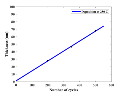
Deposition rate of ZnO at 250 oC. Substrate: Silicon 4" wafer with native oxide.

ALD window of ZnO


Uniformity across 100 mm wafer
Recipe "ZnO" Samples: 100mm ssp-Si
Results have been obtained for <100> 100 mm Si wafers with native oxide, based on ellipsometry study.
| Temperature (°C) / Number of cycles | Deposition rate (nm/s) | Average thickness (nm) | Standard deviation | Uniformity (%) |
|---|---|---|---|---|
| 100°C / 500cycles | 0.1483 | 75.67 | 1.49 | 3.26 |
| 150°C / 500cycles | 0.1954 | 95.32 | 1.32 | 2.44 |
| 200°C / 500cycles | 0.1842 | 87.97 | 0.31 | 0.63 |
| 225°C / 500cycles | 0.1622 | 81.09 | 0.45 | 1.07 |
| 250°C / 500cycles | 0.1326 | 67.92 | 1.71 | 3.82 |

Uniformity across 100mm wafer. Deposition at 100°C

Uniformity across 100mm wafer. Deposition at 150°C

Uniformity across 100mm wafer. Deposition at 200°C
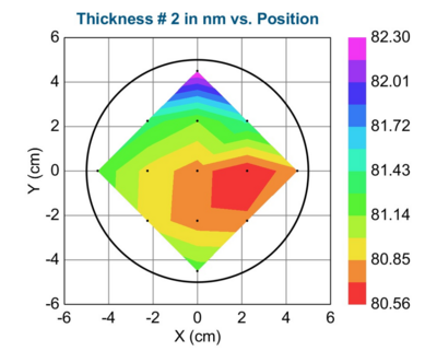
Uniformity across 100mm wafer. Deposition at 225°C

Uniformity across 100mm wafer. Deposition at 250°C


Optical functions
Results have been obtained for <100> 100 mm Si wafers with native oxide, based on ellipsometry study.
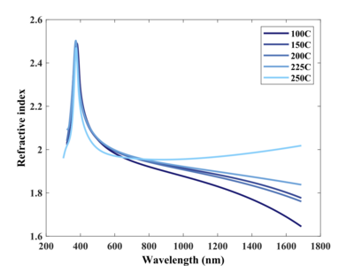
Refractive index.

Absorption coefficient.


SEM images
Images obtained using SEM inspection.
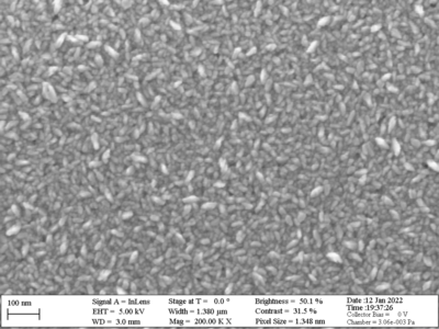
SEM image of flat surface of ZnO. Deposition at 100°C
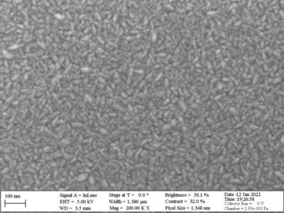
SEM image of flat surface of ZnO. Deposition at 150°C

SEM image of flat surface of ZnO. Deposition at 200°C

SEM image of flat surface of ZnO. Deposition at 225°C

SEM image of flat surface of ZnO. Deposition at 250°C
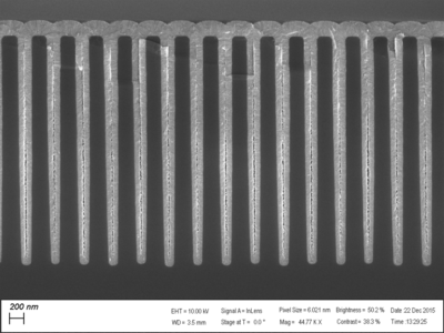
ZnO deposition example on high aspect ratio structures. "ZnOT" recipe was used.


ZnO XPS investigation for elemental trace analysis
Chemical composition of ZnO has been analyzed by XPS method. ZnO samples reveals chemically high quality films with no observable contaminations in temperature range 100 - 250 oC.
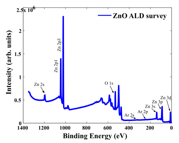
XPS survey scan of ZnO.
