Specific Process Knowledge/Characterization/KLA-Tencor Surfscan 6420: Difference between revisions
No edit summary |
|||
| (19 intermediate revisions by 4 users not shown) | |||
| Line 1: | Line 1: | ||
'''Feedback to this page''': '''[mailto:characterization@danchip.dtu.dk?Subject=Feed%20back%20from%20page%20http://http://labadviser.danchip.dtu.dk/index.php?title=Specific_Process_Knowledge/Characterization/KLA-Tencor_Surfscan_6420&action=edit&redlink=1 click here]''' | '''Feedback to this page''': '''[mailto:characterization@danchip.dtu.dk?Subject=Feed%20back%20from%20page%20http://http://labadviser.danchip.dtu.dk/index.php?title=Specific_Process_Knowledge/Characterization/KLA-Tencor_Surfscan_6420&action=edit&redlink=1 click here]''' | ||
''This page is written by DTU Nanolab internal'' | |||
==<span style="color:Red">EXPIRED. The KLA-Tencor Surfscan 6420 has has been removed from the cleanroom in April 2023. It has been replaced with the [[Specific_Process_Knowledge/Characterization/Particle_Scanner_Takano|Particle Scanner Takano]] that can be used instead.</span>== | |||
== KLA-Tencor Surfscan 6420 == | == KLA-Tencor Surfscan 6420 == | ||
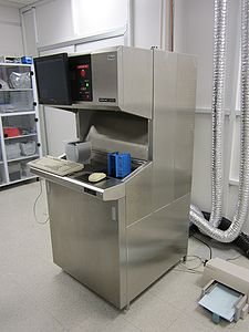
[[image:Surfscan_at_FAT.JPG|300x300px|right|thumb|The | [[image:Surfscan_at_FAT.JPG|300x300px|right|thumb|The KLA-Tencor Surfscan (at the place in California where it was refurbished).]] | ||
The KLA-Tencor is a surface analysis instrument for detecting, couting and sizing of particles, i.e. light point defects. A broad range of particles size from 0.15 µm to greater than 3 µm can be measured on a polished silicon surface with or without or epitaxial layers. The particle contamination in thin films like nitride, oxide and polymer or resist layers can also be inspected. | |||
The system will remove small surface roughness, so it will not count as particle contaminations. | |||
The system is mainly being used for quality control of the PECVDs and LPCVD nitride furnaces in the cleanroom. | |||
Users will have to contact the responsible persons (the Thin Film group), if they want to make some particle measurements. | |||
'''[http://labmanager.danchip.dtu.dk/function.php?module=Machine&view=view&mach=318 Surfscan 6420]''' | |||
== Process information == | |||
*[[Specific Process Knowledge/Characterization/KLA-Tencor Surfscan 6420/Acceptance test results|Acceptance test results]] | |||
==Overview of the performance of the Surfscan 6420 and some process related parameters== | ==Overview of the performance of the Surfscan 6420 and some process related parameters== | ||
{| border="2" cellspacing="0" cellpadding=" | {| border="2" cellspacing="0" cellpadding="2" | ||
|- | |- | ||
!style="background:silver; color:black;" align="center"|Purpose | !style="background:silver; color:black;" align="center"|Purpose | ||
| Line 22: | Line 32: | ||
|style="background:WhiteSmoke; color:black"| | |style="background:WhiteSmoke; color:black"| | ||
* | *Detecting, counting and sizing of particles (light point defects) | ||
|- | |- | ||
!style="background:silver; color:black" align="center" rowspan="3"|Performance | !style="background:silver; color:black" align="center" rowspan="3"|Performance | ||
|style="background:LightGrey; color:black"|Particles size | |style="background:LightGrey; color:black"|Particles size | ||
|style="background:WhiteSmoke; color:black"| | |style="background:WhiteSmoke; color:black"| | ||
*0. | *0.15 µm to > 3 µm | ||
|- | |- | ||
|style="background:LightGrey; color:black"|Througput | |style="background:LightGrey; color:black"|Througput | ||
| Line 35: | Line 45: | ||
|style="background:LightGrey; color:black"|Repeatbility | |style="background:LightGrey; color:black"|Repeatbility | ||
|style="background:WhiteSmoke; color:black"| | |style="background:WhiteSmoke; color:black"| | ||
*Within 1%, 1σ (mean count > 500, 0 | *Within 1%, 1σ (mean count > 500, 0.204 µm diameter latex spheres) | ||
|- | |- | ||
!style="background:silver; color:black" align="center" valign="center" rowspan=" | !style="background:silver; color:black" align="center" valign="center" rowspan="1"|Process parameter range | ||
|style="background:LightGrey; color:black"|Process Temperature | |style="background:LightGrey; color:black"|Process Temperature | ||
|style="background:WhiteSmoke; color:black"| | |style="background:WhiteSmoke; color:black"| | ||
*Room temperature | *Room temperature | ||
|- | |- | ||
!style="background:silver; color:black" align="center" valign="center" rowspan="2"|Substrates | !style="background:silver; color:black" align="center" valign="center" rowspan="2"|Substrates | ||
|style="background:LightGrey; color:black"|Batch size | |style="background:LightGrey; color:black"|Batch size | ||
|style="background:WhiteSmoke; color:black"| | |style="background:WhiteSmoke; color:black"| | ||
*1-25 100 mm wafers | *1-25 100 mm wafers | ||
*1-25 150 mm wafers | *1-25 150 mm wafers | ||
*1-25 200 mm wafers | *1-25 200 mm wafers (the loader has to be changed) | ||
|- | |- | ||
| style="background:LightGrey; color:black"|Substrate | |style="background:LightGrey; color:black"|Substrate materials allowed | ||
|style="background:WhiteSmoke; color:black"| | |style="background:WhiteSmoke; color:black"| | ||
*Silicon | |||
*Thin layers of oxide, nitride and polymer/resist | |||
|- | |- | ||
|} | |} | ||
Latest revision as of 13:58, 13 June 2023
Feedback to this page: click here
This page is written by DTU Nanolab internal
EXPIRED. The KLA-Tencor Surfscan 6420 has has been removed from the cleanroom in April 2023. It has been replaced with the Particle Scanner Takano that can be used instead.
KLA-Tencor Surfscan 6420

The KLA-Tencor is a surface analysis instrument for detecting, couting and sizing of particles, i.e. light point defects. A broad range of particles size from 0.15 µm to greater than 3 µm can be measured on a polished silicon surface with or without or epitaxial layers. The particle contamination in thin films like nitride, oxide and polymer or resist layers can also be inspected. The system will remove small surface roughness, so it will not count as particle contaminations.
The system is mainly being used for quality control of the PECVDs and LPCVD nitride furnaces in the cleanroom.
Users will have to contact the responsible persons (the Thin Film group), if they want to make some particle measurements.
Process information
| Purpose |
| |
|---|---|---|
| Performance | Particles size |
|
| Througput |
| |
| Repeatbility |
| |
| Process parameter range | Process Temperature |
|
| Substrates | Batch size |
|
| Substrate materials allowed |
|
