Specific Process Knowledge/Etch/Etching of Silicon Oxide/SiO2 etch using ASE/ICP recipe for SiO2: Difference between revisions
Jump to navigation
Jump to search
No edit summary |
No edit summary |
||
| Line 5: | Line 5: | ||
|-style="background:Black; color:White" | |-style="background:Black; color:White" | ||
! Parameter | ! Parameter | ||
|Recipe name: ''' | |Recipe name: '''SiO2_ICP''' | ||
|- | |- | ||
|Coil Power [W] | |Coil Power [W] | ||
|150 | |150 | ||
|- | |- | ||
|Platen Power [W] | |Platen Power [W] | ||
|25 | |25 | ||
|- | |- | ||
|Platen temperature [<sup>o</sup>C] | |Platen temperature [<sup>o</sup>C] | ||
|20 | |20 | ||
|- | |- | ||
|C<sub>4</sub>F<sub>8</sub> flow [sccm] | |C<sub>4</sub>F<sub>8</sub> flow [sccm] | ||
|36 | |36 | ||
|- | |- | ||
|H<sub>2</sub> flow [sccm] | |H<sub>2</sub> flow [sccm] | ||
|13 | |13 | ||
|- | |- | ||
|He flow [sccm] | |He flow [sccm] | ||
|0 | |0 | ||
|- | |- | ||
|Pressure [mTorr] | |Pressure [mTorr] | ||
|2.5 | |2.5 | ||
|- | |- | ||
Revision as of 14:22, 15 May 2023
This recipe was taken from the ICP Metal etch, with a slight difference in the platen temperature.
| Parameter | Recipe name: SiO2_ICP |
|---|---|
| Coil Power [W] | 150 |
| Platen Power [W] | 25 |
| Platen temperature [oC] | 20 |
| C4F8 flow [sccm] | 36 |
| H2 flow [sccm] | 13 |
| He flow [sccm] | 0 |
| Pressure [mTorr] | 2.5 |
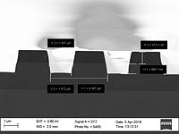
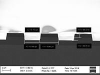
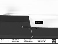
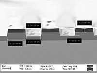
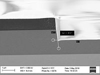
Results when etching a piece of wafer on a Si carrier
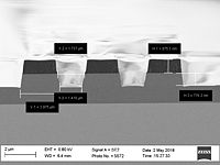
Results when etching a whole wafer on an Al carrier
| Material to be etched | Recipe: SiO2_ICP |
|---|---|
| Etch rate in SiO2 | 22.1 nm/min |
| Etch rate in resist (MIR) | 16.6 nm/min |
| Selectivity (SiO2:resist) | 1.3 |
| Profile Images | 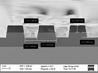 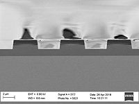 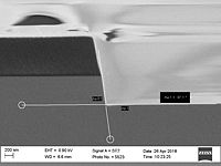
|
| Material to be etched | Recipe: SIO2_ICP | Testing othe etch rate in nitride |
|---|---|---|
| Etch rate in SiO2 | 22.1 nm/min | ? |
| Etch rate in PECVD nitride | . | 20.8nm/min (kabi@nanolab 20190301) - ~0nm/min (ecsj@nanolab 20210729) |
| Etch rate in LPCVD nitride | . | 23.7 nm/min in the middle, 17 nm/min close to the edge |
| Etch rate in resist (MIR) | 12.5 nm/min | 13.9 nm/min |
| Selectivity (SiO2:resist) | 1.8 | 1.9 |
| Etch rate in silicon |
| |
| Profile Images |
