Specific Process Knowledge/Characterization/XPS/XPS Depth profiling: Difference between revisions
| (18 intermediate revisions by 2 users not shown) | |||
| Line 1: | Line 1: | ||
= | '''Feedback to this page''': '''[mailto:labadviser@nanolab.dtu.dk?Subject=Feed%20back%20from%20page%20http://labadviser.nanolab.dtu.dk/index.php?title=Specific_Process_Knowledge/Characterization/XPS/XPS_Depth_profiling click here]''' | ||
<!--Checked for updates on 24/8-2021. ok/ jmli--> | |||
<!-- Page reviewed 8/5-2023 jmli --> | |||
{{Author-jmli1}} | |||
=Depth profiling= | |||
The photoelectrons have a very short inelastic mean free path - this means that although generated at roughly equal numbers from the surface to deep inside the sample, only the photoelectrons emerging from the topmost layers will survive the passage to the surface unscattered. Photoelectrons that have undergone inelastic collisions will have lost a fraction of their kinetic energy - and hence no longer contribute to the intensity of the peak but will find itself in the rise in background signal on the left side of the peak in the spectrum (corresponding to lower kinetic energy). | |||
This means that only atoms sitting in the topmost nanometers of the sample contribute to the intensity of the peak making the technique very surface sensitive. To access deeper layers of the sample one can use the argon ion gun to sputter off the surface layers of the sample - and then record a new set of spectra. A series with cycles of measurement with subsequent sputtering can be set up in this way creating a depth profile of the sample. | |||
== Example: Si wafer thin layers of oxide, nitride and polysilicon == | |||
Below is an example of a depth profile. The sample is a sandwich of: | |||
* Silicon wafer | |||
* Silicon oxide | |||
* Silicon nitride | |||
* Polysilicon | |||
[[File:profile sandwich 3.PNG|700px|{{photo1}}]] | |||
In the | In the spectra required to make such a depth profile, one can distinguish the various chemical environments of silicon depending on whether it is bonded to: | ||
* Silicon as in the bulk (oxidation state 0). | |||
* Oxygen, either fully oxidized (oxidation state IV) in SiO<sub>2</sub> or in intermediate states with a mixture of silicon and oxygen bonds (oxidation state I, II and III) | |||
* Nitrogen, also fully oxidized (oxidation state IV) | |||
and plot their atomic percentages along with the percentages of oxygen and nitrogen. | |||
Latest revision as of 14:31, 8 May 2023
Feedback to this page: click here
Unless otherwise stated, all content on this page was created by Jonas Michael-Lindhard, DTU Nanolab
Depth profiling
The photoelectrons have a very short inelastic mean free path - this means that although generated at roughly equal numbers from the surface to deep inside the sample, only the photoelectrons emerging from the topmost layers will survive the passage to the surface unscattered. Photoelectrons that have undergone inelastic collisions will have lost a fraction of their kinetic energy - and hence no longer contribute to the intensity of the peak but will find itself in the rise in background signal on the left side of the peak in the spectrum (corresponding to lower kinetic energy).
This means that only atoms sitting in the topmost nanometers of the sample contribute to the intensity of the peak making the technique very surface sensitive. To access deeper layers of the sample one can use the argon ion gun to sputter off the surface layers of the sample - and then record a new set of spectra. A series with cycles of measurement with subsequent sputtering can be set up in this way creating a depth profile of the sample.
Example: Si wafer thin layers of oxide, nitride and polysilicon
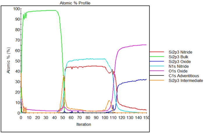
Below is an example of a depth profile. The sample is a sandwich of:
- Silicon wafer
- Silicon oxide
- Silicon nitride
- Polysilicon
In the spectra required to make such a depth profile, one can distinguish the various chemical environments of silicon depending on whether it is bonded to:
- Silicon as in the bulk (oxidation state 0).
- Oxygen, either fully oxidized (oxidation state IV) in SiO2 or in intermediate states with a mixture of silicon and oxygen bonds (oxidation state I, II and III)
- Nitrogen, also fully oxidized (oxidation state IV)
and plot their atomic percentages along with the percentages of oxygen and nitrogen.

