Specific Process Knowledge/Etch/Etching of Silicon Nitride/Etch of Silicon Nitride using RIE: Difference between revisions
Jump to navigation
Jump to search
No edit summary |
|||
| (12 intermediate revisions by 4 users not shown) | |||
| Line 1: | Line 1: | ||
For a general introduction to RIE at | '''Feedback to this page''': '''[mailto:labadviser@nanolab.dtu.dk?Subject=Feed%20back%20from%20page%20http://labadviser.nanolab.dtu.dk/index.php/Specific_Process_Knowledge/Etch/Etching_of_Silicon_Nitride/Etch_of_Silicon_Nitride_using_RIE click here]''' <br> | ||
{{CC-DTU}} | |||
=<span style="color:#FF0000"> Both RIE's (RIE1 and RIE2) for silicon based etching have been decommissioned </span> = | |||
* <span style="color:#FF0000"> This information is save because it might be valuable as inspiration for other dry etch systems. | |||
For a general introduction to RIE at DTU Nanolab see [[Specific Process Knowledge/Etch/RIE (Reactive Ion Etch)|RIE (Reactive Ion Etch)]] | |||
Etching of silicon nitride using RIE can be done with several recipes. It can be etched by our standard silicon etch recipe: OH_PolyA which is based on SF6. It can also be etched using the recipe 1Nitride which is based on CHF3. The difference of these two etches has not been investigate in details. Look in the table below to see what we know | Etching of silicon nitride using RIE can be done with several recipes. It can be etched by our standard silicon etch recipe: OH_PolyA which is based on SF6. It can also be etched using the recipe 1Nitride which is based on CHF3. The difference of these two etches has not been investigate in details. Look in the table below to see what we know | ||
| Line 25: | Line 30: | ||
|. | |. | ||
|8 sccm | |8 sccm | ||
| | |43 sccm | ||
|38 mTorr | |38 mTorr | ||
|50 W | |50 W | ||
| Line 38: | Line 43: | ||
! valign="top" |Etch rate | ! valign="top" |Etch rate | ||
!valign="top" |Anisotropy | !valign="top" |Anisotropy | ||
!valign="top" |Selectivity to resist | !valign="top" |Selectivity to nitride:resist | ||
!valign="top" |Selectivity to oxide | !valign="top" |Selectivity to nitride:oxide | ||
!valign="top" |Selectivity to silicon | !valign="top" |Selectivity to nitride:silicon | ||
!valign="top" |Comments | !valign="top" |Comments | ||
|- valign="top" | |- valign="top" | ||
|'''OH_PolyA''' | |'''OH_PolyA''' | ||
|10-20% | |10-20% | ||
|0.05 µm/min | |0.05 µm/min ''(tested before 2014)'' | ||
|? | |? | ||
|~1:1 | |~1:1 | ||
|~ | |~2-3:1 | ||
|~1:13 | |~1:13 | ||
| | |. | ||
|-valign="top" | |-valign="top" | ||
|'''BGE-NITR''' | |'''BGE-NITR''' | ||
|10-20% | |10-20% | ||
|0.04 µm/min | |0.04 µm/min ''(tested before 2014)'' | ||
|Expected to be very anisotropic - not verified | |Expected to be very anisotropic - not verified | ||
|? | |? | ||
| Line 61: | Line 66: | ||
|Especially good to remove nitride on one side of the wafer avoiding getting anything etched on the back side. | |Especially good to remove nitride on one side of the wafer avoiding getting anything etched on the back side. | ||
|} | |} | ||
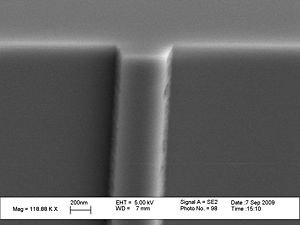
[[image:bc_5_7 jpeg.jpg|300x300px|left|thumb|SEM picture shoving the etch profile for a wafer with 150 nm nitride that has been etched in RIE1 which has been decommissioned but similar results are expected on RIE2. The wafer has been etched for 3.5 min with the recipe "BGE_NITR" (pressure increased to 42 mTorr), and most of the wafer (>99 %) has been etched. The structures are made with e-beam lithography, and the Al etch mask has been removed before the SEM inspection. Wafer tilted 45 degrees.]] | |||
Latest revision as of 12:05, 24 March 2023
Feedback to this page: click here
Unless otherwise stated, the contact of this page is done by DTU internal
Both RIE's (RIE1 and RIE2) for silicon based etching have been decommissioned
- This information is save because it might be valuable as inspiration for other dry etch systems.
For a general introduction to RIE at DTU Nanolab see RIE (Reactive Ion Etch)
Etching of silicon nitride using RIE can be done with several recipes. It can be etched by our standard silicon etch recipe: OH_PolyA which is based on SF6. It can also be etched using the recipe 1Nitride which is based on CHF3. The difference of these two etches has not been investigate in details. Look in the table below to see what we know
Some RIE recipes for etching of silicon nitride:
| Name | SF6 flow | O2 flow | CHF3 flow | N2 flow | Pressure | Power |
|---|---|---|---|---|---|---|
| OH_PolyA | 32 sccm | 8 sccm | . | . | 80 mTorr | 30 W |
| BGE-NITR | . | . | 8 sccm | 43 sccm | 38 mTorr | 50 W |
Expected result using the above RIE recipes for etching of silicon nitride:
You should be aware that the result can deviate quit a lot from what is written here depending on ex. the mask loading.
| Name | Tested with mask load: | Etch rate | Anisotropy | Selectivity to nitride:resist | Selectivity to nitride:oxide | Selectivity to nitride:silicon | Comments |
|---|---|---|---|---|---|---|---|
| OH_PolyA | 10-20% | 0.05 µm/min (tested before 2014) | ? | ~1:1 | ~2-3:1 | ~1:13 | . |
| BGE-NITR | 10-20% | 0.04 µm/min (tested before 2014) | Expected to be very anisotropic - not verified | ? | ~1:1 | ~1:1 | Especially good to remove nitride on one side of the wafer avoiding getting anything etched on the back side. |

SEM picture shoving the etch profile for a wafer with 150 nm nitride that has been etched in RIE1 which has been decommissioned but similar results are expected on RIE2. The wafer has been etched for 3.5 min with the recipe "BGE_NITR" (pressure increased to 42 mTorr), and most of the wafer (>99 %) has been etched. The structures are made with e-beam lithography, and the Al etch mask has been removed before the SEM inspection. Wafer tilted 45 degrees.