Specific Process Knowledge/Thin film deposition/Deposition of Silicon Oxide/IBSD of SiO2: Difference between revisions
No edit summary |
No edit summary |
||
| (One intermediate revision by the same user not shown) | |||
| Line 1: | Line 1: | ||
'''Feedback to this page''': '''[mailto:labadviser@nanolab.dtu.dk?Subject=Feed%20back%20from%20page%20http://labadviser.nanolab.dtu.dk/index.php/Specific_Process_Knowledge/Thin_film_deposition/Deposition_of_Silicon_Oxide/IBSD_of_SiO2 click here]''' | '''Feedback to this page''': '''[mailto:labadviser@nanolab.dtu.dk?Subject=Feed%20back%20from%20page%20http://labadviser.nanolab.dtu.dk/index.php/Specific_Process_Knowledge/Thin_film_deposition/Deposition_of_Silicon_Oxide/IBSD_of_SiO2 click here]''' <br> | ||
{{CC1}} | |||
| Line 151: | Line 151: | ||
==Other results== | ==Other results== | ||
===Roughness of the surface=== | ===Roughness of the surface=== | ||
Measured with the Optical profiler - PSI mode (on one sample from the acceptance test): Sa= 0. | Measured with the Optical profiler - PSI mode (on one sample from the acceptance test): Sa= 0.6 nm | ||
===Uniformity and break down voltage ''by Mathias Engholm 2016-11-29''=== | ===Uniformity and break down voltage ''by Mathias Engholm 2016-11-29''=== | ||
Latest revision as of 11:56, 24 March 2023
Feedback to this page: click here
Unless otherwise stated, this page is written by DTU Nanolab internal
Go to 'IBE/IBSD Ionfab 300' equipment page
Acceptance test for SiO2 deposition (2011) on IBE/IBSD Ionfab 300+)
| . | Acceptance Criteria |
Acceptance Result 1 |
Acceptance Result 2 |
|---|---|---|---|
| Substrate information |
|
|
|
| Material to be deposited |
The purpose of the SiO2 is to be part of a mirror: <br\> 5 quarter wavelength pairs of <br\> SiO2 <br\> TiO2 <br\> Extra quarter wavelength layer of <br\> TiO2 <br\> 5 quarter wavelength pairs of <br\> SiO2 <br\> TiO2 <br\> Design wavelength (for refractive indices and layer thicknesses): 1300nm <br\> The acceptance criteria is set up for the single SiO2 and TiO2 layers. <br\> Five runs in a row for each material. |
|
|
| Deposition thickness |
|
|
|
| Deposition rate |
|
One standard deviation |
Only made once |
| Thickness uniformity |
|
|
|
| Reproducibility |
|
|
|
| Stress |
|
|
|
| Refractive index | . |
|
|
| Recipe 1 | Recipe 2 | |
|---|---|---|
| Platen angle | 15 degrees | 10 degrees |
| Platen rotation speed | 20 rpm | 20 rpm |
| Ar(N) flow | 4 sccm | 4 sccm |
| Ar(dep. source) flow | 9 sccm | 8 sccm |
| I(N) | 310 mA | 320 mA |
| Power | 675 W | 700 W |
| I(B) | 310 mA | 280 mA |
| V(B) | 1200 V | 1100 V |
| Vacc(B) | 400 V | 400 V |
| Deposition time | 29 min | 37 min |
Other results
Roughness of the surface
Measured with the Optical profiler - PSI mode (on one sample from the acceptance test): Sa= 0.6 nm
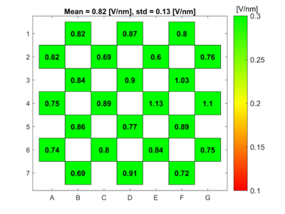
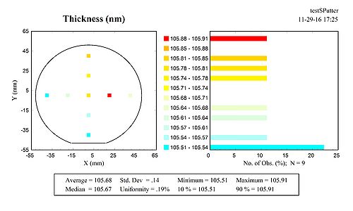
Uniformity and break down voltage by Mathias Engholm 2016-11-29
Mathias made 105.62nm SiO2 on a test silicon wafer and on his sample wafer. The sample wafer had gold/Cr on the surface and that had to be electrically isolated. The uniformity over the wafer of the oxide was 0.19% over 9 points - this is better than he has achieved when oxidizing in a furnace. He anodic bonded the wafer without problems. He measured the breakdown voltage and got 0.82+/+ 0.13 V/nm over 24 points. This is just as good as the oxide from the furnaces. Before his deposition he ran a 20 min heat up and 40min dummy deposition to clean the target. This was done with a bright new target and with the small deposition grids mounted.

