Specific Process Knowledge/Etch/ICP Metal Etcher/silicon oxide/By Peixiong/images CF4: Difference between revisions
No edit summary |
|||
| (5 intermediate revisions by the same user not shown) | |||
| Line 1: | Line 1: | ||
'''''All images on this page has been created by Peixiong Shi, DTU Nanolab''''' <br> | |||
==Images stepper_6A1_feb262013_step9== | ==Images stepper_6A1_feb262013_step9== | ||
<gallery caption="6A1_feb262013_step9" widths="200px" heights="150px" perrow="4"> | <gallery caption="6A1_feb262013_step9" widths="200px" heights="150px" perrow="4"> | ||
| Line 13: | Line 14: | ||
image:10mm from wf edge_089.jpg|wafer edge | image:10mm from wf edge_089.jpg|wafer edge | ||
image:10mm from wf edge_090.jpg|wafer edge | image:10mm from wf edge_090.jpg|wafer edge | ||
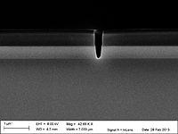
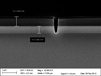
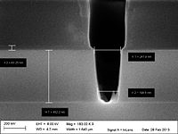
image:10mm from wf edge_091.jpg|wafer edge | image:10mm from wf edge_091.jpg|Position of the scanning: wafer edge | ||
image:10mm from wf edge_092.jpg|wafer edge | image:10mm from wf edge_092.jpg|wafer edge | ||
image:10mm from wf edge_093.jpg|wafer edge | image:10mm from wf edge_093.jpg|wafer edge | ||
Latest revision as of 15:21, 22 March 2023
All images on this page has been created by Peixiong Shi, DTU Nanolab
Images stepper_6A1_feb262013_step9
- 6A1_feb262013_step9
-
-
-
-


Images stepper_6A4_feb262013_step9
- 6A4_feb262013_step9
-
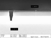
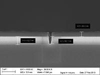
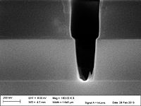
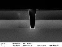
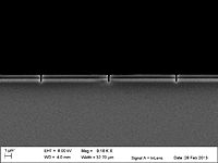
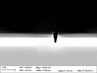 wafer edge
 -
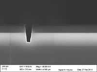
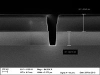
 wafer edge
 -
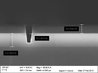
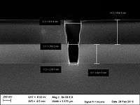
 wafer edge
 -
 wafer edge
 -
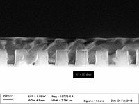
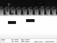
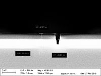
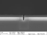
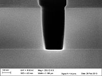
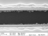
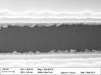
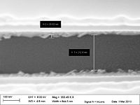
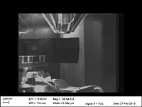 Position of the scanning: wafer edge
 -
 wafer edge
 -
 wafer edge
 -
-
-
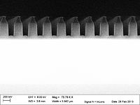
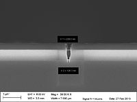
 wafer center
 -
 wafer center
 -
 wafer center
 -
 wafer center


Images Stepper_6A5_feb272013
- 6A5_feb262013 step9 and step10
-
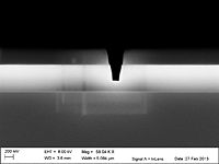
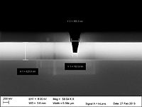
 Wafer edge
 -
 Wafer edge
 -
 Wafer edge
 -
 Wafer edge
 -
 Wafer edge
 -
 Wafer edge
 -
 Wafer center
 -
 Wafer center
 -
 Wafer center
 -
 Wafer center
 -
 Wafer center
 -
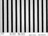
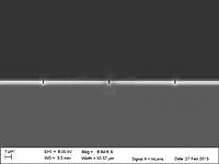
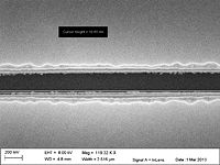
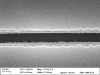 Top view
 -
 Top view
 -
 Top view
 -
 Top view
 -
 Top view
 -
 Top view


images 3
- 6A1_feb262013_step9