Specific Process Knowledge/Back-end processing/Disco Saw: Difference between revisions
| (23 intermediate revisions by the same user not shown) | |||
| Line 5: | Line 5: | ||
The dicers at DTU Nanolab is placed in room 157 on the first floor in bldg. 346. Please notice that this is not a cleanroom and that the dicing process is very dirty. | The dicers at DTU Nanolab is placed in room 157 on the first floor in bldg. 346. Please notice that this is not a cleanroom and that the dicing process is very dirty. | ||
<!-- | |||
[[Image:Disco_DAD_321_Dicer.jpg|thumb|Dicer positioned on 1. floor bldg 346 room 157]] | |||
[[Image:DAD_3241_picture.jpg|thumb|Dicer positioned on 1. floor bldg 346 room 157]] | |||
--> | |||
In general it is ''not allowed'' to bring back your samples into the Cleanroom. You need approval from DTU Nanolab staff to do this. Your samples have to be thoroughly cleaned in the gowning area and get a Piranha cleaning. You will only be allowed to use a limited number of tools for the processing after dicing. | In general it is ''not allowed'' to bring back your samples into the Cleanroom. You need approval from DTU Nanolab staff to do this. Your samples have to be thoroughly cleaned in the gowning area and get a Piranha cleaning. You will only be allowed to use a limited number of tools for the processing after dicing. | ||
[[File:IMG_20230228_112922.jpg|thumb|800px|Dicers positioned on 1. floor bldg 346 room 157]] | |||
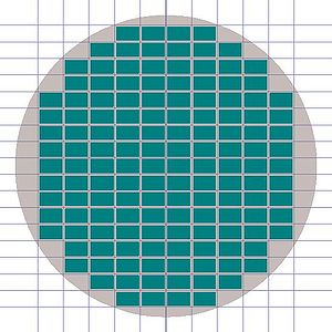
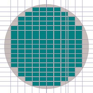
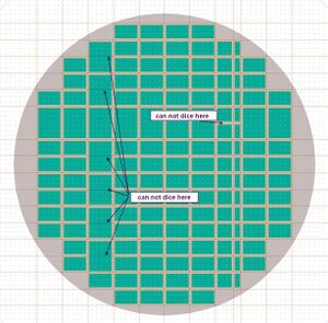
Please consider your layout of dies on your wafer. The dicer can only cut straight lines across the wafer and you can not end a line in the middle of the wafer. | Please consider your layout of dies on your wafer. The dicer can only cut straight lines across the wafer and you can not end a line in the middle of the wafer. | ||
Please see the illustrations for a good and a bad design. | Please see the illustrations for a good and a bad design. | ||
{| cellpadding="2" style="border: 2px solid darkgray; | {| cellpadding="2" style="border: 2px solid darkgray;" | ||
! width=" | ! width="300" | | ||
! width=" | ! width="300" | | ||
! width=" | ! width="300" | | ||
|- align="center" | |- align="center" | ||
| '''GOOD design - simple''' || '''GOOD design - complex''' || <span style="color:red">'''BAD design'''</span> | | '''GOOD design - simple''' || '''GOOD design - complex''' || <span style="color:red">'''BAD design'''</span> | ||
|- border="1" align="center" | |- border="1" align="center" | ||
|[[Image:Good design 2.jpg| | |[[Image:Good design 2.jpg|300x300px|Good design]] || [[Image:Good design 3.jpg|300x300px|Good design]] || [[Image:Bad design 1b.jpg|300x300px|BAD design]] | ||
| | | | ||
|- align="center" | |- align="center" | ||
| '''GOOD design - simple''' || '''GOOD design - complex''' || <span style="color:red">'''BAD design'''</span> | | '''GOOD design - simple''' || '''GOOD design - complex''' || <span style="color:red">'''BAD design'''</span> | ||
|- | |||
| || drawings by Jesper Hanberg, DTU Nanolab || | |||
|} | |} | ||
== Process information == | |||
'''The user manual, user APV, technical information and contact information can be found in LabManager:''' | *'''The user manual, user APV, technical information and contact information can be found in LabManager:''' | ||
<!-- remember to remove the type of documents that are not present --> | <!-- remember to remove the type of documents that are not present --> | ||
<!-- give the link to the equipment info page in LabManager: --> | <!-- give the link to the equipment info page in LabManager: --> | ||
*[http://labmanager. | **[http://labmanager.nanolab.dtu.dk/function.php?module=Machine&view=view&mach=168 DAD 321 Saw in LabManager] | ||
*[http://labmanager. | **[http://labmanager.nanolab.dtu.dk/function.php?module=Machine&view=view&mach=489 DAD 3241 Saw in LabManager] | ||
*[[Specific Process Knowledge/Back-end processing/Disco Saw#Comparing dicing parameters for different materials |Comparing dicing parameters for different materials]] | *[[Specific Process Knowledge/Back-end processing/Disco Saw#Comparing dicing parameters for different materials |Comparing dicing parameters for different materials]] | ||
*[[Specific Process Knowledge/Back-end processing/Disco Saw#Images of diced samples |Images of diced samples]] | *[[Specific Process Knowledge/Back-end processing/Disco Saw#Images of diced samples |Images of diced samples]] | ||
*Dicing work sheet: [[Media:Dicing. | *Dicing work sheet: [[Media:Dicing Work Sheet v2.docx |Dicing Work Sheet v2.docx]] Fill out before requesting dicing. | ||
===Overview of the performance Disco | ===Overview of the performance Disco DAD 321 and DAD 3241 Dicer=== | ||
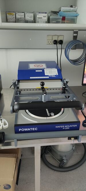
[[Image:IMG 20230228 113020.jpg|thumb|Wafer mounter for DAD 3241]] | |||
{| border="2" cellspacing="0" cellpadding="10" | {| border="2" cellspacing="0" cellpadding="10" | ||
|- | |- | ||
!style="background:silver; color:black;" align="left"|Purpose | !style="background:silver; color:black;" align="left" rowspan="2"|Machine | ||
|style="background:LightGrey; color:black"| | |style="background:LightGrey; color:black"|Name | ||
|style="background:WhiteSmoke; color:black"| | |||
DAD 321 (old) | |||
|style="background:WhiteSmoke; color:black"| | |||
DAD 3241 (new 2021) | |||
|- | |||
|style="background:LightGrey; color:black"|Operation | |||
|style="background:WhiteSmoke; color:black"| | |||
*Keyboard | |||
*F-key menu driven | |||
*BW screen | |||
|style="background:WhiteSmoke; color:black"| | |||
*Touch screen | |||
*Guided menu | |||
*Color screen | |||
|- | |||
!style="background:silver; color:black;" align="left" rowspan="2"|Purpose | |||
|style="background:LightGrey; color:black"|Main usage | |||
|style="background:WhiteSmoke; color:black"| | |style="background:WhiteSmoke; color:black"| | ||
Dicing Borofloat and Fused Silica wafers | |||
|style="background:WhiteSmoke; color:black"| | |style="background:WhiteSmoke; color:black"| | ||
Dicing Silicon wafers | |||
|- | |- | ||
|style="background:LightGrey; color:black"|Wafer type | |||
|style="background:LightGrey; color:black"| | |||
|style="background:WhiteSmoke; color:black"| | |style="background:WhiteSmoke; color:black"| | ||
*'''Pyrex/Borofloat''' | *'''Pyrex/Borofloat''' | ||
*'''Fused Silica''' | *'''Fused Silica''' | ||
*'''Silicon bonded to Pyrex/Borofloat''' | *'''Silicon bonded to Pyrex/Borofloat''' | ||
*'''Silicon bonded to Silicon''' | *'''Silicon bonded to Silicon''' | ||
* Other materials - ask | |||
*Pure Silicon samples | *Pure Silicon samples | ||
|style="background:WhiteSmoke; color:black"| | |style="background:WhiteSmoke; color:black"| | ||
| Line 69: | Line 88: | ||
*Silicon bonded to Silicon | *Silicon bonded to Silicon | ||
*Silicon bonded to Pyrex/Borofloat | *Silicon bonded to Pyrex/Borofloat | ||
* Other materials - ask | |||
|- | |- | ||
!style="background:silver; color:black" align="left" valign="top" rowspan="5"|Performance | !style="background:silver; color:black" align="left" valign="top" rowspan="5"|Performance | ||
| Line 75: | Line 95: | ||
192 mm | 192 mm | ||
|style="background:WhiteSmoke; color:black"| | |style="background:WhiteSmoke; color:black"| | ||
210 mm | |||
|- | |- | ||
|style="background:LightGrey; color:black"|X-axis cut speed | |style="background:LightGrey; color:black"|X-axis cut speed | ||
| Line 81: | Line 101: | ||
0.1 - 300 mm/sec | 0.1 - 300 mm/sec | ||
|style="background:WhiteSmoke; color:black"| | |style="background:WhiteSmoke; color:black"| | ||
0.1 - 800 mm/sec | |||
|- | |- | ||
|style="background:LightGrey; color:black"|Y-axis cutting range | |style="background:LightGrey; color:black"|Y-axis cutting range | ||
| Line 87: | Line 107: | ||
162 mm | 162 mm | ||
|style="background:WhiteSmoke; color:black"| | |style="background:WhiteSmoke; color:black"| | ||
210 mm | |||
|- | |- | ||
|style="background:LightGrey; color:black"|Y-axis index step | |style="background:LightGrey; color:black"|Y-axis index step | ||
| Line 93: | Line 113: | ||
0.0002 mm | 0.0002 mm | ||
|style="background:WhiteSmoke; color:black"| | |style="background:WhiteSmoke; color:black"| | ||
0. | 0.0001 mm | ||
|- | |- | ||
|style="background:LightGrey; color:black"|Y-axis single error | |style="background:LightGrey; color:black"|Y-axis single error | ||
| Line 99: | Line 119: | ||
0.003 or less | 0.003 or less | ||
|style="background:WhiteSmoke; color:black"| | |style="background:WhiteSmoke; color:black"| | ||
0. | 0.002 or less | ||
|- | |- | ||
|- | |- | ||
!style="background:silver; color:black" align="left" valign="top" rowspan="2"|Substrates | !style="background:silver; color:black" align="left" valign="top" rowspan="2"|Substrates | ||
| Line 123: | Line 136: | ||
*Thick metal (>0.75 mm) | *Thick metal (>0.75 mm) | ||
*III-V samples | *III-V samples | ||
|- | |||
!style="background:silver; color:black" align="left" valign="top" rowspan="2"|Accessories | |||
| style="background:LightGrey; color:black"|Accessories for wafer handling | |||
|style="background:WhiteSmoke; color:black"| | |||
*Manual wafer mounter for blue tape | |||
|style="background:WhiteSmoke; color:black"| | |||
*Manual wafer mounter for tape with backside foil (Powatec P200) | |||
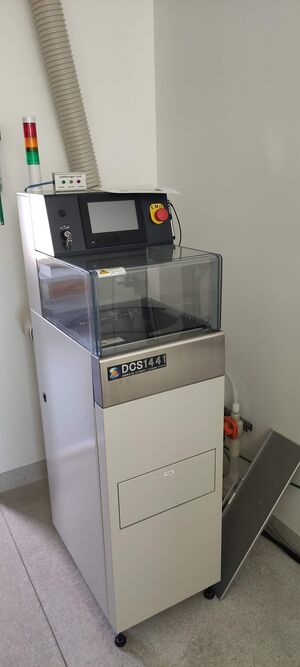
*Automatic Wafer cleaning station (Disco DCS 1441) | |||
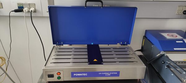
*UV curing station (Powatec U200) | |||
|- | |- | ||
|} | |} | ||
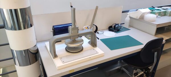
[[Image:IMG 20230228 113101.jpg|thumb|600px|left|Wafer mounting table for DAD 321]] | |||
[[Image:IMG 20230228 113035.jpg|thumb|600px|UV curing/Tape release]] | |||
<br clear="all" /> | <br clear="all" /> | ||
===Comparing dicing parameters for different materials '''DAD 321'''=== | ===Comparing dicing parameters for different materials '''DAD 321'''=== | ||
[[Image:IMG 20230228 113045.jpg|300px|thumb|Wafer cleaning station DCS 1441]] | |||
Do not mix blades for the DAD 321 with the blades for the DAD 3241. They have different outer diameters | Do not mix blades for the DAD 321 with the blades for the DAD 3241. They have different outer diameters | ||
{| border="2" cellspacing="0" cellpadding="4 | {| border="2" cellspacing="0" cellpadding="4" | ||
! | ! | ||
!Silicon | !Silicon | ||
| Line 173: | Line 198: | ||
Do not mix blades for the DAD 321 with the blades for the DAD 3241. They have different outer diameters | Do not mix blades for the DAD 321 with the blades for the DAD 3241. They have different outer diameters | ||
{| border="2" cellspacing="0" cellpadding="4 | {| border="2" cellspacing="0" cellpadding="4" | ||
! | ! | ||
!Silicon | !Silicon | ||
| Line 203: | Line 228: | ||
|- | |- | ||
|} | |} | ||
<!-- | |||
This is not a typical dice line! | |||
===Images of diced samples=== | ===Images of diced samples=== | ||
[[Image:Dicetest_001.jpg|300x300px|thumb|Si V-groove diced with ZH05 blade |left]] | [[Image:Dicetest_001.jpg|300x300px|thumb|Si V-groove diced with ZH05 blade |left]] | ||
--> | |||
Revision as of 13:05, 28 February 2023
Feedback to this page: click here
Disco Automatic dicing saw, model DAD321 (old) and DAD3241 (new 2021)
The dicers feature versatile processing capabilities, compact designs, and high precision and reliability. Users perform workpiece loading, alignment, and unloading manually.
The dicers at DTU Nanolab is placed in room 157 on the first floor in bldg. 346. Please notice that this is not a cleanroom and that the dicing process is very dirty.
In general it is not allowed to bring back your samples into the Cleanroom. You need approval from DTU Nanolab staff to do this. Your samples have to be thoroughly cleaned in the gowning area and get a Piranha cleaning. You will only be allowed to use a limited number of tools for the processing after dicing.

Please consider your layout of dies on your wafer. The dicer can only cut straight lines across the wafer and you can not end a line in the middle of the wafer. Please see the illustrations for a good and a bad design.
| GOOD design - simple | GOOD design - complex | BAD design | |
 |
 |
|
|
| GOOD design - simple | GOOD design - complex | BAD design | |
| drawings by Jesper Hanberg, DTU Nanolab |
Process information
- The user manual, user APV, technical information and contact information can be found in LabManager:
- Comparing dicing parameters for different materials
- Images of diced samples
- Dicing work sheet: Dicing Work Sheet v2.docx Fill out before requesting dicing.
Overview of the performance Disco DAD 321 and DAD 3241 Dicer
| Machine | Name |
DAD 321 (old) |
DAD 3241 (new 2021) |
|---|---|---|---|
| Operation |
|
| |
| Purpose | Main usage |
Dicing Borofloat and Fused Silica wafers |
Dicing Silicon wafers |
| Wafer type |
|
| |
| Performance | X-axis cutting range |
192 mm |
210 mm |
| X-axis cut speed |
0.1 - 300 mm/sec |
0.1 - 800 mm/sec | |
| Y-axis cutting range |
162 mm |
210 mm | |
| Y-axis index step |
0.0002 mm |
0.0001 mm | |
| Y-axis single error |
0.003 or less |
0.002 or less | |
| Substrates | Substrate size |
up to 6" |
up to 8" |
| Layers that can't be diced |
|
| |
| Accessories | Accessories for wafer handling |
|
|
Comparing dicing parameters for different materials DAD 321
Do not mix blades for the DAD 321 with the blades for the DAD 3241. They have different outer diameters
| Silicon | Pyrex or bonded Si/Pyrex | |
|---|---|---|
| Bladetype | HUB Blade ZH05 (27HEEF) | HUBless Blade B1A862 |
| Blade width | 50 µm | 150 µm |
| Cutlinewidth | 60 µm | 180 - 200 µm |
| Recommended feed speed | Up to 20 mm/sec | Up to 2 mm/sec (0.5 mm/sec) |
| Recommended dice depth | Set blade height to 200µm (preferred). This leaves 125µm uncut since blue tape is 75µm. It is possible to cut through the sample. |
Do not cut deeper than 500 µm in each pass (for fused Silica and SiC 200 µm). If you have thicker wafers then use several passes decreasing the blade height for each pass. |
| Max. sample thickness | 1.5 mm | 2.0 mm |
Comparing dicing parameters for different materials DAD 3241
Do not mix blades for the DAD 321 with the blades for the DAD 3241. They have different outer diameters
| Silicon | Other materials | |
|---|---|---|
| Bladetype | HUB Blade | Ask! (HUBless) |
| Blade width | 50 µm | ask |
| Cutlinewidth | 50 µm | ask |
| Recommended feed speed | Up to 40 mm/sec | ask |
| Recommended dice depth | We usually cut all way through the wafer with a blade height of 50µm (preferred). |
ask! |
| Max. sample thickness | 1.5 mm | 2.0 mm |
