Specific Process Knowledge/Thin film deposition/Deposition of Chromium/Sputtering of Cr in Cluster Lesker PC3: Difference between revisions
No edit summary |
No edit summary |
||
| (3 intermediate revisions by the same user not shown) | |||
| Line 1: | Line 1: | ||
This page presents the results of Cr deposition using DC sputtering in Sputter- | '''Feedback to this page''': '''[mailto:labadviser@nanolab.dtu.dk?Subject=Feed%20back%20from%20page%20http://labadviser.nanolab.dtu.dk/index.php/Specific_Process_Knowledge/Thin_film_deposition/Deposition_of_Chromium/Sputtering_of_Cr_in_Cluster_Lesker_PC3 click here]''' | ||
<i>This page is written by <b>Evgeniy Shkondin @DTU Nanolab</b> if nothing else is stated. <br> | |||
All images and photos on this page belongs to <b>DTU Nanolab</b>.<br> | |||
The fabrication and characterization described below were conducted in <b>2021-2022 by Evgeniy Shkondin</b>.<br></i> | |||
This page presents the results of Cr deposition using DC sputtering in [[Specific Process Knowledge/Thin film deposition/Cluster-based multi-chamber high vacuum sputtering deposition system|Sputter-System Metal-Nitride(PC3)]], now commonly known as "Cluster Lesker". The deposition target is Cr 3-inch. Source #2 (DC/p-DC) was used. | |||
The fabrication and characterization described below were conducted in <i>2022 by Evgeniy Shkondin, DTU Nanolab</i>. The focus of the study was the deposition conditions and uniformity check across 150mm wafer. | The fabrication and characterization described below were conducted in <i>2022 by Evgeniy Shkondin, DTU Nanolab</i>. The focus of the study was the deposition conditions and uniformity check across 150mm wafer. | ||
The prepared film was investigated by the X-ray | The prepared film was investigated by the [[Specific Process Knowledge/Characterization/XRD/XRD_SmartLab|X-ray rfelectivity method]]. The process recipe is following: | ||
Recipe: | Recipe: | ||
| Line 26: | Line 33: | ||
=X-ray reflectivity analysis= | =X-ray reflectivity analysis= | ||
X-ray analysis | [[Specific Process Knowledge/Characterization/XRD/XRD_SmartLab|X-ray reflectivity analysis]] of Cr samples have been performed to investigate the thicknesses, roughness, and density profiles. | ||
The scans has been obtained using Rigaku XRD SmartLab equipment. The voltage and current settings for the Cu X-ray tube were standard 40kV and 30mA. The incident optics contained a IPS (incident parallel slit) adaptor with 5 ° Soller slit. Other slits: IS=0.03mm RS1=0.03mm and RS2=0.075mm. Step size: 0.01 and measurement time - 5s for each point. Fitting procesure was performed using commercial GlobalFit software assuming the model based on Si substrates with native oxide followed by the deposited Cr film with thin oxides and moisture surfaces. The results are summarized in a tables below. | The scans has been obtained using Rigaku XRD SmartLab equipment. The voltage and current settings for the Cu X-ray tube were standard 40kV and 30mA. The incident optics contained a IPS (incident parallel slit) adaptor with 5 ° Soller slit. Other slits: IS=0.03mm RS1=0.03mm and RS2=0.075mm. Step size: 0.01 and measurement time - 5s for each point. Fitting procesure was performed using commercial GlobalFit software assuming the model based on Si substrates with native oxide followed by the deposited Cr film with thin oxides and moisture surfaces. The results are summarized in a tables below. | ||
| Line 41: | Line 48: | ||
{| border="2" cellspacing="2" cellpadding="3" colspan="16" | {| border="2" cellspacing="2" cellpadding="3" colspan="16" | ||
|bgcolor="#eed5d2" |'''XRR results for Cr layer deposited at 3 mTorr, 350W, 30s.''' | |bgcolor="#eed5d2" |'''XRR results for Cr layer deposited at 3 mTorr, 350W, 30s. 150mm wafer''' | ||
|- | |- | ||
| | | | ||
Latest revision as of 20:36, 18 February 2023
Feedback to this page: click here
This page is written by Evgeniy Shkondin @DTU Nanolab if nothing else is stated.
All images and photos on this page belongs to DTU Nanolab.
The fabrication and characterization described below were conducted in 2021-2022 by Evgeniy Shkondin.
This page presents the results of Cr deposition using DC sputtering in Sputter-System Metal-Nitride(PC3), now commonly known as "Cluster Lesker". The deposition target is Cr 3-inch. Source #2 (DC/p-DC) was used.
The fabrication and characterization described below were conducted in 2022 by Evgeniy Shkondin, DTU Nanolab. The focus of the study was the deposition conditions and uniformity check across 150mm wafer.
The prepared film was investigated by the X-ray rfelectivity method. The process recipe is following:
Recipe:
- Power unit: Power Supply 5 (DC)
- Gun: Src2
- Deposition type: DC
- Gas: Ar
- Power used: 350 W
- Pressure: 3 mTorr
- Temperature: 20°C (no heating)
- Deposition time: 30 s
- Observed DC bias: 412V
- Deposition Rate: 0.468 nm/s
Deposition rate for Cr is a bit higher in PC3 compared to PC1 at the same power, This is due to the shorter distance between the source and the wafer (12.5 cm in PC3 vs. 15 cm in PC1).
X-ray reflectivity analysis
X-ray reflectivity analysis of Cr samples have been performed to investigate the thicknesses, roughness, and density profiles.
The scans has been obtained using Rigaku XRD SmartLab equipment. The voltage and current settings for the Cu X-ray tube were standard 40kV and 30mA. The incident optics contained a IPS (incident parallel slit) adaptor with 5 ° Soller slit. Other slits: IS=0.03mm RS1=0.03mm and RS2=0.075mm. Step size: 0.01 and measurement time - 5s for each point. Fitting procesure was performed using commercial GlobalFit software assuming the model based on Si substrates with native oxide followed by the deposited Cr film with thin oxides and moisture surfaces. The results are summarized in a tables below.
- X-ray reflectivity results. Uniformity
-
 Cr thin film deposited at 350 W, 3 mTorr and 20°C. Center of the 150mm wafer.
 -
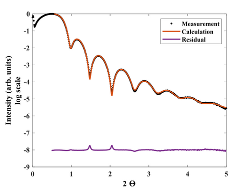 Cr thin film deposited at 350 W, 3 mTorr and 20°C. Edge of the 150mm wafer.


| XRR results for Cr layer deposited at 3 mTorr, 350W, 30s. 150mm wafer | |||||||||||||||||||||||||||||||||||||||||||||||||||||||||||||||||
| |||||||||||||||||||||||||||||||||||||||||||||||||||||||||||||||||

| Fitting parameters | ||||||||||||||||
|---|---|---|---|---|---|---|---|---|---|---|---|---|---|---|---|---|
| Sample | Moisture | CrOx | Cr | Si native oxide | Si substrate | Fitting parameters | ||||||||||
| Delta | Beta | Delta | Beta | Delta | Beta | Delta | Beta | Delta | Beta | Intensity | Background | Fitting area () | R | |||
| Center | 3.8129E-6 | 8.8542E-8 | 1.6021E-5 | 1.1148E-6 | 2.0572E-5 | 2.1158E-6 | 7.7460E-6 | 1.7987E-7 | 7.5860E-6 | 1.7616E-7 | 1.19063E+000 | 1.00877E-006 | 0.4775 - 5.0080 | 0.00695 | 0.00081 | |
| Edge | 2.3226E-6 | 5.3933E-8 | 1.1725E-5 | 8.1591E-6 | 2.0899E-5 | 2.1494E-6 | 7.7588E-6 | 1.8017E-7 | 7.5860E-6 | 1.7616E-7 | 1.29242E+000 | 1.48454E-006 | 0.4775 - 5.0080 | 0.01019 | 0.00170 | |

