Specific Process Knowledge/Back-end processing/Polisher CMP: Difference between revisions
No edit summary |
|||
| (7 intermediate revisions by 2 users not shown) | |||
| Line 1: | Line 1: | ||
'''Unless anything else is stated, everything on this page, text and pictures are made by DTU Nanolab.''' | |||
'''All links to Kemibrug (SDS) and Labmanager Including APV and QC requires login.''' | |||
'''Feedback to this page''': '''[mailto:labadviser@danchip.dtu.dk?Subject=Feed%20back%20from%20page%20http://labadviser.danchip.dtu.dk/index.php/Specific_Process_Knowledge/Back-end_processing/Polisher_CMP click here]''' | '''Feedback to this page''': '''[mailto:labadviser@danchip.dtu.dk?Subject=Feed%20back%20from%20page%20http://labadviser.danchip.dtu.dk/index.php/Specific_Process_Knowledge/Back-end_processing/Polisher_CMP click here]''' | ||
| Line 6: | Line 11: | ||
== Polisher (CMP) == | == Polisher (CMP) == | ||
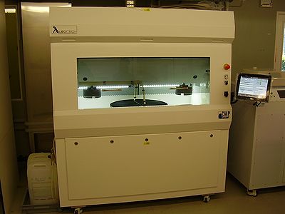
[[image:Cmp_picture.jpg|400px|right|thumb|The Logitech PM5 Polisher/Lapper]] | [[image:Cmp_picture.jpg|400px|right|thumb|The Logitech PM5 Polisher/Lapper in cleanroom A-5]] | ||
The Logitech Orbis Polisher (CMP) is for polishing wafers (removing material in the nm range) it is not for thinning down wafers or other substrates. | The Logitech Orbis Polisher (CMP) is for polishing wafers (removing material in the nm range) it is not for thinning down wafers or other substrates. After CMP it is recommended to use the '''[http://labadviser.nanolab.dtu.dk/index.php/Specific_Process_Knowledge/Wafer_cleaning/Post_CMP_Cleaner Post CMP Cleaner]''' to clean the sample for slurry residues left by the CMP. | ||
| Line 16: | Line 21: | ||
<!-- give the link to the equipment info page in LabManager: --> | <!-- give the link to the equipment info page in LabManager: --> | ||
[http://labmanager.danchip.dtu.dk/function.php?module=Machine&view=view&mach=430 The Logitech Orbis (CMP) in LabManager] | [http://labmanager.danchip.dtu.dk/function.php?module=Machine&view=view&mach=430 The Logitech Orbis (CMP) in LabManager] | ||
==Equipment performance and process related parameters== | ==Equipment performance and process related parameters== | ||
| Line 28: | Line 32: | ||
!style="background:silver; color:black;" align="center" width="60"|Purpose | !style="background:silver; color:black;" align="center" width="60"|Purpose | ||
|style="background:LightGrey; color:black"| | |style="background:LightGrey; color:black"| | ||
Polishing of | |||
|style="background:WhiteSmoke; color:black"| | |style="background:WhiteSmoke; color:black"| | ||
*Silicon | *Silicon | ||
* | *SiO2 | ||
<!-- |style="background:WhiteSmoke; color:black"| | <!-- |style="background:WhiteSmoke; color:black"| | ||
*Purpose 1 | *Purpose 1 | ||
| Line 41: | Line 42: | ||
|- | |- | ||
!style="background:silver; color:black" align="center" valign="center" rowspan="2"|Performance | !style="background:silver; color:black" align="center" valign="center" rowspan="2"|Performance | ||
|style="background:LightGrey; color:black"| | |style="background:LightGrey; color:black"| 20x20mm substrate | ||
|style="background:WhiteSmoke; color:black"| | |style="background:WhiteSmoke; color:black"| | ||
*Removal rate: | *Removal rate: 400nm/min | ||
*Thickness accuracy: +/- | *Thickness accuracy: +/- ? µm | ||
*Thickness homogeneity: +/- | *Thickness homogeneity: +/- ? µm | ||
*Roughness: +/- ? µm | *Roughness: +/- ? µm | ||
<!-- |style="background:WhiteSmoke; color:black"| | <!-- |style="background:WhiteSmoke; color:black"| | ||
| Line 52: | Line 53: | ||
*Performance range 3 --> | *Performance range 3 --> | ||
|- | |- | ||
|style="background:LightGrey; color:black"| | |style="background:LightGrey; color:black"|100mm substrate | ||
|style="background:WhiteSmoke; color:black"| | |style="background:WhiteSmoke; color:black"| | ||
*Removal rate: ~ | *Removal rate: ~ 60 nm/min | ||
*Thickness accuracy: ? µm | *Thickness accuracy: ? µm | ||
*Thickness homogeneity: ? µm | *Thickness homogeneity: ? µm | ||
| Line 70: | Line 71: | ||
*Chemcloth Polishing Cloths | *Chemcloth Polishing Cloths | ||
|- | |- | ||
|style="background:LightGrey; color:black"|Rotation | |style="background:LightGrey; color:black"|Rotation | ||
|style="background:WhiteSmoke; color:black"| | |style="background:WhiteSmoke; color:black"| | ||
* | *Plate | ||
* | *Head/Puck | ||
|- | |- | ||
|style="background:LightGrey; color:black"|Arm sweep | |style="background:LightGrey; color:black"|Arm sweep | ||
Latest revision as of 16:21, 6 February 2023
Unless anything else is stated, everything on this page, text and pictures are made by DTU Nanolab.
All links to Kemibrug (SDS) and Labmanager Including APV and QC requires login.
Feedback to this page: click here
Polisher (CMP)

The Logitech Orbis Polisher (CMP) is for polishing wafers (removing material in the nm range) it is not for thinning down wafers or other substrates. After CMP it is recommended to use the Post CMP Cleaner to clean the sample for slurry residues left by the CMP.
The user manual, user APV, technical information and contact information can be found in LabManager:
The Logitech Orbis (CMP) in LabManager
| Equipment | Polisher/Lapper | |
|---|---|---|
| Purpose |
Polishing of |
|
| Performance | 20x20mm substrate |
|
| 100mm substrate |
| |
| Process parameter range | Polishing liquid |
|
| Polishing cloths |
| |
| Rotation |
| |
| Arm sweep |
| |
| Substrates | Sample size |
|
| Allowed materials |
| |
