Specific Process Knowledge/Etch/Etching of Silicon/Si etch using RIE1 or RIE2: Difference between revisions
No edit summary |
|||
| (46 intermediate revisions by 4 users not shown) | |||
| Line 1: | Line 1: | ||
'''Feedback to this page''': '''[mailto:labadviser@nanolab.dtu.dk?Subject=Feed%20back%20from%20page%20http://labadviser.danchip.dtu.dk/index.php/Specific_Process_Knowledge/Etch/Etching_of_Silicon/Si_etch_using_RIE1_or_RIE2 click here]''' <br> | |||
{{CC-bghe1}} | |||
=<span style="color:#FF0000"> Both RIE's (RIE1 and RIE2) for silicon based etching has been decommissioned </span> = | |||
RIE (Reactive Ion Etch) can be used for etching silicon - both crystalline and polycrystalline silicon. The etch can be isotropic or anisotropic with vertical sidewalls depending on the process recipe and the masking material and geometry. The Si is etched by flour radicals that are created from SF<sub>6</sub>(g) in a RF generated plasma. | RIE (Reactive Ion Etch) can be used for etching silicon - both crystalline and polycrystalline silicon. The etch can be isotropic or anisotropic with vertical sidewalls depending on the process recipe and the masking material and geometry. The Si is etched by flour radicals that are created from SF<sub>6</sub>(g) in a RF generated plasma. | ||
== | ==Most used recipe:== | ||
{| border="1" cellspacing="2" cellpadding="2" colspan="3" | |||
|bgcolor="#98FB98" |'''Quality Controle (QC) for RIE2''' | |||
* | |- | ||
* | | | ||
*[http://labmanager.danchip.dtu.dk/d4Show.php?id=1389&mach=18 The QC procedure for RIE2]<br> | |||
*[http://www.labmanager.danchip.dtu.dk/view_binary.php?type=data&mach=19 The newest QC data for RIE2] | |||
{| {{table}} | |||
| align="center" | | |||
{| border="1" cellspacing="1" cellpadding="2" align="center" style="width:200px" | |||
== | ! QC Recipe: | ||
! OH_POLYA | |||
|- | |||
| SF<sub>6</sub> flow | |||
|32 sccm | |||
|- | |||
|O<sub>2</sub> flow | |||
|8 sccm | |||
|- | |||
|Pressure | |||
|80 mTorr | |||
|- | |||
|RF-power | |||
|30 W | |||
|- | |||
|Etch Load | |||
|50% | |||
|- | |||
|} | |||
| align="center" valign="top"| | |||
{| border="2" cellspacing="1" cellpadding="2" align="center" style="width:500px" | |||
!QC limits | |||
!RIE2 | |||
|- | |||
|Etch rate in Si | |||
|358 - 554 nm/min | |||
|- | |||
|Non-uniformity | |||
|<11.0 % | |||
|- | |||
|} | |||
|- | |||
|} | |||
|} | |||
Hint: When using resist as masking material then do a 15 sec. buffer dip before the etch to remove any residual of resist which is normally left after the photo lithography step. A short O<sub>2</sub> plasma will also do. | |||
{| border="1" cellspacing="1" cellpadding="2" align="left" | {| border="1" cellspacing="1" cellpadding="2" align="left" | ||
| Line 35: | Line 75: | ||
{| border="2" cellspacing="1" cellpadding="3" align="center" | {| border="2" cellspacing="1" cellpadding="3" align="center" | ||
! | ! | ||
!Expected results in RIE1 | !Expected results in RIE1 (has been decommissioned) | ||
!Expected results in RIE2 | !Expected results in RIE2 | ||
! RIE2 results for almost 100% load ''by Yannick Seis@nbi.ku.dk May 2017'' (4min etch) | |||
|- | |- | ||
|Etch rate in Si | |Etch rate in Si | ||
|~0.40 µm/min | |style="background:WhiteSmoke; color:silver"| | ||
~0.40 µm/min | |||
|~0.45 µm/min | |~0.45 µm/min | ||
|0.35µm/min (center)<br> | |||
0.30 (half way)<br> | |||
0.28 (edge) | |||
|- | |- | ||
|Etch rate in Si<sub>3</sub>N<sub>4</sub> | |Etch rate in Si<sub>3</sub>N<sub>4</sub> | ||
| | |. | ||
|~0.05 µm/min | |~0.05 µm/min | ||
|- | |- | ||
|Etch rate in SiO<sub>2</sub> | |Etch rate in SiO<sub>2</sub> | ||
| | |. | ||
|~0.02 µm/min | |~0.02 µm/min | ||
|. | |||
|- | |- | ||
|Etch rate in photoresist | |||
|style="background:WhiteSmoke; color:silver"| | |||
~0.06 µm/min | |||
|~0.05 µm/min | |||
|. | |||
|} | |} | ||
<br clear="all" /> | |||
===The etch load affects the results=== | |||
The etching results are dependent on the mask geometry, primarily the etch load (meaning the area fraction of the silicon substrate that is exposed to the plasma). | |||
To illustrate this, you can see on the images below the effect of etch load on the results of the OH_PolyA recipe. The first one has a very low load of 1-10% and the second has a load of 50%. It can be seen that the sidewalls are closer to vertical with 50% load than with 1-10 % load. Also the etch rate is effected by the load. | |||
''' | '''Etch load <50%:''' | ||
*The etch rate is approximately the same. | *The etch rate is approximately the same. | ||
*The etch profile is more isotropic | *The etch profile is more isotropic | ||
''' | '''Etch load >50%:''' | ||
*The etch rate decreases almost linear with the exposed area. The etch rate of a 100% load has once been seen to be reduced to about 65% of the etch rate of a 60% load. | *The etch rate decreases almost linear with the exposed area. The etch rate of a 100% load has once been seen to be reduced to about 65% of the etch rate of a 60% load. | ||
*The etch profile is not expected to change significantly. | *The etch profile is not expected to change significantly. | ||
[[image: | [[image:RIE1 OHPOLYA TRAVKA10 200um00.jpg|370x370px|thumb|left|RIE1: OH_Polya on etch load 10% Etch rate:~0.61 µm/min]] | ||
[[image:RIE1 | [[image:RIE1 OHPOLYA TRAVKA50 200um01.jpg|370x370px|thumb|none|RIE1: OH_Polya on etch load 50% Etch rate:~0.49 µm/min]] | ||
<br clear="all" /> | |||
===RIE Travka results - Silicon etch rate and profile as function of etch load=== | |||
More information about the etch rate and profile as function of the etch load for RIE1 and RIE2 can be found here: | |||
[[/Specific Process Knowledge/Etch/Etching of Silicon/Si etch using RIE1 or RIE2/RIE1 Travka results|RIE1 Travka results - RIE1 has been decommissioned]] | |||
[[/Specific Process Knowledge/Etch/Etching of Silicon/Si etch using RIE1 or RIE2/RIE2 Travka results|RIE2 Travka results]] | |||
A description of the Travka mask set can be found here: | |||
[[Specific Process Knowledge/Lithography/UVExposure/travka|Travka mask set]] | |||
==Etch of small structures== | ==Etch of small structures== | ||
=== | |||
===RIE2:=== | |||
A Design Of Experiment (DOE) has been performed. Here is a short summary: | A Design Of Experiment (DOE) has been performed. Here is a short summary: | ||
{| border=" | {| border="2" cellspacing="1" cellpadding="2" align="none" | ||
! Recipe: | ! Recipe: | ||
! | ! | ||
| Line 87: | Line 154: | ||
|- | |- | ||
|Pressure | |Pressure | ||
| | |36 mTorr | ||
|- | |- | ||
|RF-power | |RF-power | ||
| Line 93: | Line 160: | ||
|- | |- | ||
|} | |} | ||
More details on the DOE can be seen here: "DOE | |||
[[image:DOE_RIE2_Si_Angle_O2_CHF3.jpg|300x300px|thumb|none|Angle of sidewall on 1.5 µm trenches]] | |||
<br clear="all" /> | |||
More details on the DOE can be seen here: "DOE RIE2 silicon etch of small structures" (not available yet). | |||
Here are a few images of some of the single experiments in the DOE. The width of the trenches are roughly 1.5µm: | Here are a few images of some of the single experiments in the DOE. The width of the trenches are roughly 1.5µm: | ||
{| border="1" cellspacing="1" cellpadding="2" | {| border="1" cellspacing="1" cellpadding="2" | ||
! | ! | ||
[[image: | [[image:DOE_RIE2_Si_O2245_CHF310.jpg|100x100px|thumb|center|O2:24.5sccm CHF3:10sccm]] | ||
! | ! | ||
[[image: | [[image:DOE_RIE2_Si_O229_CHF315.jpg|100x100px|thumb|center|O2:29sccm CHF3:15sccm]] | ||
! | ! | ||
[[image: | [[image:DOE_RIE2_Si_O220_CHF35.jpg|100x100px|thumb|center|O2:20sccm CHF3:5sccm]] | ||
]] | |||
|} | |} | ||
More details on the DOE can be seen here: "DOE RIE2 silicon etch of small structures": [[Media:RIE1_of_Silicon_20070306.pdf| DOE of RIE2]] | |||
=== | ===RIE1: RIE1 HAS BEEN DECOMMISSIONED=== | ||
A Design Of Experiment (DOE) has been performed. Here is a short summary: | A Design Of Experiment (DOE) has been performed. Here is a short summary: | ||
{| border="1" cellspacing="1" cellpadding="2" align="none" | |||
{| border="1" cellspacing="1" cellpadding="2" align=" | |||
! Recipe: | ! Recipe: | ||
! | ! | ||
| Line 127: | Line 197: | ||
|- | |- | ||
|Pressure | |Pressure | ||
| | |31-41 mTorr | ||
|- | |- | ||
|RF-power | |RF-power | ||
| Line 133: | Line 203: | ||
|- | |- | ||
|} | |} | ||
More details on the DOE can be seen here: "DOE | |||
[[image:RIE1_Si_Angle_O2_CHF3.jpg|300x300px|thumb|none|Angle of sidewall on 1.5 µm trenches - independent on pressure within the given pressure range]] | |||
<br clear="all" /> | |||
More details on the DOE can be seen here: "DOE RIE1 silicon etch of small structures": [[Media:RIE1_of_Silicon_20070306.pdf]] | |||
Here are a few images of some of the single experiments in the DOE. The width of the trenches are roughly 1.5µm: | Here are a few images of some of the single experiments in the DOE. The width of the trenches are roughly 1.5µm: | ||
{| border="1" cellspacing="1" cellpadding="2" | {| border="1" cellspacing="1" cellpadding="2" | ||
! | ! | ||
[[image: | [[image:DOE RIE1 O2245 CHF310 P36.jpg|100x100px|thumb|center|O2:24.5sccm CHF3:10sccm Pressure:36mTorr]] | ||
! | ! | ||
[[image: | [[image:DOE RIE1 O229 CHF315 P31.jpg|100x100px|thumb|center|O2:29sccm CHF3:15sccm Pressure:31mTorr]] | ||
! | ! | ||
[[image: | [[image:DOE RIE1 O220 CHF35 P31.jpg|100x100px|thumb|center|O2:20sccm CHF3:5sccm Pressure:31mTorr | ||
]] | |||
|} | |} | ||
<br clear="all" /> | |||
Latest revision as of 15:22, 6 February 2023
Feedback to this page: click here
This page is written by Berit Herstrøm @ DTU Nanolab (BGHE) if nothing else is stated
Both RIE's (RIE1 and RIE2) for silicon based etching has been decommissioned
RIE (Reactive Ion Etch) can be used for etching silicon - both crystalline and polycrystalline silicon. The etch can be isotropic or anisotropic with vertical sidewalls depending on the process recipe and the masking material and geometry. The Si is etched by flour radicals that are created from SF6(g) in a RF generated plasma.
Most used recipe:
| Quality Controle (QC) for RIE2 | ||||||||||||||||||||
|
Hint: When using resist as masking material then do a 15 sec. buffer dip before the etch to remove any residual of resist which is normally left after the photo lithography step. A short O2 plasma will also do.
| Recipe: | OH_POLYA |
|---|---|
| SF6 flow | 32 sccm |
| O2 flow | 8 sccm |
| Pressure | 80 mTorr |
| RF-power | 30 W |
| Expected results in RIE1 (has been decommissioned) | Expected results in RIE2 | RIE2 results for almost 100% load by Yannick Seis@nbi.ku.dk May 2017 (4min etch) | |
|---|---|---|---|
| Etch rate in Si |
~0.40 µm/min |
~0.45 µm/min | 0.35µm/min (center) 0.30 (half way) |
| Etch rate in Si3N4 | . | ~0.05 µm/min | |
| Etch rate in SiO2 | . | ~0.02 µm/min | . |
| Etch rate in photoresist |
~0.06 µm/min |
~0.05 µm/min | . |
The etch load affects the results
The etching results are dependent on the mask geometry, primarily the etch load (meaning the area fraction of the silicon substrate that is exposed to the plasma).
To illustrate this, you can see on the images below the effect of etch load on the results of the OH_PolyA recipe. The first one has a very low load of 1-10% and the second has a load of 50%. It can be seen that the sidewalls are closer to vertical with 50% load than with 1-10 % load. Also the etch rate is effected by the load.
Etch load <50%:
- The etch rate is approximately the same.
- The etch profile is more isotropic
Etch load >50%:
- The etch rate decreases almost linear with the exposed area. The etch rate of a 100% load has once been seen to be reduced to about 65% of the etch rate of a 60% load.
- The etch profile is not expected to change significantly.
RIE Travka results - Silicon etch rate and profile as function of etch load
More information about the etch rate and profile as function of the etch load for RIE1 and RIE2 can be found here:
RIE1 Travka results - RIE1 has been decommissioned
A description of the Travka mask set can be found here:
Etch of small structures
RIE2:
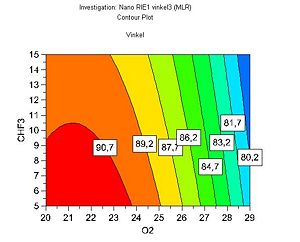
A Design Of Experiment (DOE) has been performed. Here is a short summary:
| Recipe: | |
|---|---|
| SF6 flow | 30 sccm |
| O2 flow | 20-29 sccm |
| CHF3 flow | 5-15 scmm |
| Pressure | 36 mTorr |
| RF-power | 20 W |
More details on the DOE can be seen here: "DOE RIE2 silicon etch of small structures" (not available yet).
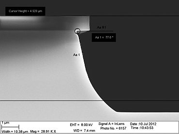
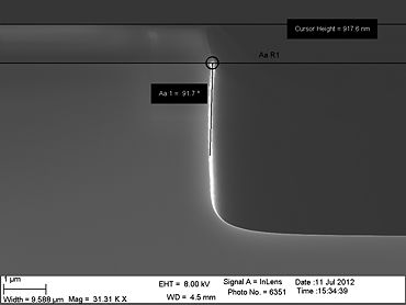
Here are a few images of some of the single experiments in the DOE. The width of the trenches are roughly 1.5µm:
More details on the DOE can be seen here: "DOE RIE2 silicon etch of small structures": DOE of RIE2
RIE1: RIE1 HAS BEEN DECOMMISSIONED
A Design Of Experiment (DOE) has been performed. Here is a short summary:
| Recipe: | |
|---|---|
| SF6 flow | 30 sccm |
| O2 flow | 20-29 sccm |
| CHF3 flow | 5-15 scmm |
| Pressure | 31-41 mTorr |
| RF-power | 20 W |
More details on the DOE can be seen here: "DOE RIE1 silicon etch of small structures": Media:RIE1_of_Silicon_20070306.pdf
Here are a few images of some of the single experiments in the DOE. The width of the trenches are roughly 1.5µm:


