Specific Process Knowledge/Etch/Etching of Silicon Oxide/SiO2 etch using RIE1 or RIE2: Difference between revisions
(New page: RIE (Reactive Ion Etch) can be used for etching silicon oxide. The etch is anisotropic with vertical or angled sidewalls depending on the process recipe and the masking material and geomet...) |
No edit summary |
||
| (50 intermediate revisions by 3 users not shown) | |||
| Line 1: | Line 1: | ||
'''Feedback to this page''': '''[mailto:labadviser@nanolab.dtu.dk?Subject=Feed%20back%20from%20page%20http://labadviser.nanolab.dtu.dk/index.php/Specific_Process_Knowledge/Etch/Etching_of_Silicon_Oxide/SiO2_etch_using_RIE1_or_RIE2 click here]''' <br> | |||
{{CC-bghe1}} <br> | |||
=<span style="color:#FF0000"> Both RIE's (RIE1 and RIE2) for silicon based etching has been decommissioned </span> = | |||
RIE (Reactive Ion Etch) can be used for etching silicon oxide. The etch is anisotropic with vertical or angled sidewalls depending on the process recipe and the masking material and geometry. The SiO<sub>2</sub> is etched by flour radicals assisted by ion bombardment. | RIE (Reactive Ion Etch) can be used for etching silicon oxide. The etch is anisotropic with vertical or angled sidewalls depending on the process recipe and the masking material and geometry. The SiO<sub>2</sub> is etched by flour radicals assisted by ion bombardment. | ||
==The substrate:== | ==The substrate:== | ||
Must be a wafer of 4" or below or small pieces, not higher than about 2mm. The system can be set up for 6", please ask 2 weeks in advance. | |||
==The silicon can be masked by these materials:== | ==The silicon can be masked by these materials:== | ||
| Line 10: | Line 14: | ||
*Silicon Nitride | *Silicon Nitride | ||
*Aluminium | *Aluminium | ||
*Other metals if they cover less than 5% of the wafer area. | |||
*Other metals if they cover less than 5% of the wafer area | |||
==Most used | ==Most used recipes:== | ||
===QC results=== | |||
{| border="1" cellspacing="2" cellpadding="2" colspan="3" | |||
|bgcolor="#98FB98" |'''Quality Controle (QC) for RIE2 - oxide etch''' | |||
|- | |||
| | |||
*[http://labmanager.danchip.dtu.dk/d4Show.php?id=1389&mach=18 The QC procedure for RIE2]<br> | |||
*[http://www.labmanager.danchip.dtu.dk/view_binary.php?type=data&mach=19 The newest QC data for RIE2] | |||
{| {{table}} | |||
| align="center" | | |||
{| border="1" cellspacing="1" cellpadding="2" align="center" style="width:200px" | |||
! QC Recipe: | |||
! QCOXIDE | |||
|- | |||
| CF<sub>4</sub> flow | |||
| 14 sccm | |||
|- | |||
|CHF<sub>3</sub> flow | |||
| 26 sccm | |||
|- | |||
|Pressure | |||
|100 mTorr | |||
|- | |||
|RF-power | |||
|60 W | |||
|- | |||
|Etch Load | |||
|100% | |||
|- | |||
|} | |||
| align="center" valign="top"| | |||
{| border="2" cellspacing="1" cellpadding="2" align="center" style="width:500px" | |||
!QC limits | |||
!RIE2 | |||
|- | |||
|Etch rate in Si | |||
|6 - 17 nm/min | |||
|- | |||
|Non-uniformity | |||
|<±13.5% | |||
|- | |||
|} | |||
|- | |||
|} | |||
|} | |||
===Resist as masking material:=== | |||
{| border="1" cellspacing="1" cellpadding="2" align="left" | {| border="1" cellspacing="1" cellpadding="2" align="left" | ||
! Recipe: | ! Recipe: | ||
! 1SiO2mre | ! 1SiO2mre | ||
|- | |- | ||
|Masking material | |||
|Photoresist | |||
|- | |||
| CF<sub>4</sub> flow | | CF<sub>4</sub> flow | ||
|14 sccm | |14 sccm | ||
| Line 35: | Line 87: | ||
{| border="2" cellspacing="1" cellpadding="3" align="center" | {| border="2" cellspacing="1" cellpadding="3" align="center" | ||
! | ! | ||
!Expected results in RIE1 | !Expected results in RIE1 (has been decommissioned) | ||
!Expected results in RIE2 | !Expected results in RIE2 | ||
|- | |- | ||
|Etch rate in SiO<sub>2</sub> | |Etch rate in SiO<sub>2</sub> | ||
|~20-30 nm/min | |style="background:WhiteSmoke; color:silver"| | ||
~20-30 nm/min | |||
|~20-30 nm/min | |~20-30 nm/min | ||
|- | |- | ||
| Line 47: | Line 100: | ||
|- | |- | ||
|Etch rate in P-Si (when used as mask) | |Etch rate in P-Si (when used as mask) | ||
|~30 nm/min | |style="background:WhiteSmoke; color:silver"| | ||
~30 nm/min | |||
|~30 nm/min | |~30 nm/min | ||
|- | |- | ||
|Etch rate in Si ( | |Etch rate in Si | ||
|Expected <2 nm/min | (etching down to Si) | ||
|style="background:WhiteSmoke; color:silver"| | |||
Expected <2 nm/min | |||
|Expected <2 nm/min | |Expected <2 nm/min | ||
|- | |- | ||
|} | |} | ||
mre:mask resist | mre:mask resist | ||
===PolySilicon as masking material=== | |||
{| border="1" cellspacing="1" cellpadding="2" align="left" | |||
! Recipe: | |||
! 1SiO2msi | |||
|- | |||
|Masking material | |||
|Silicon | |||
|- | |||
| CF<sub>4</sub> flow | |||
|8 sccm | |||
|- | |||
|CHF<sub>3</sub> flow | |||
|40 sccm | |||
|- | |||
|Pressure | |||
|150 mTorr | |||
|- | |||
|RF-power | |||
|150 W | |||
|- | |||
|} | |||
{| border="2" cellspacing="1" cellpadding="3" align="center" | |||
! | |||
!Expected results in RIE1 (HAS BEEN DECOMMISSIONED) | |||
!Expected results in RIE2 | |||
|- | |||
|Etch rate in SiO<sub>2</sub> | |||
|style="background:WhiteSmoke; color:silver"| | |||
~70-80 nm/min | |||
|~70-80 nm/min | |||
|- | |||
|Etch rate in Si<sub>3</sub>N<sub>4</sub> | |||
|? | |||
|? | |||
|- | |||
|Etch rate in P-Si (when used as mask) | |||
|style="background:WhiteSmoke; color:silver"| | |||
~20-30 nm/min | |||
|~20-30 nm/min | |||
|- | |||
|Etch rate in Si | |||
(etching down to Si) | |||
|? | |||
|? | |||
|- | |||
|Images | |||
|style="background:WhiteSmoke; color:silver"| | |||
[[/Images of 1SiO2mSi with p-Si mask|Etches with p-Si as masking material]] | |||
|[[/Images of 1SiO2mSi with p-Si mask|Etches with p-Si as masking material]] | |||
|- | |||
|} | |||
msi:mask silicon | |||
The recipe: 1SiO2bre (se below) can also be used with p-Si as masking material. | |||
===Burned resist as masking material (developed for waveguides by ''Haiyan Ou @DTU Photonics''):=== | |||
{| border="1" cellspacing="1" cellpadding="2" align="left" | |||
! Recipe: | |||
! 1SiO2mbr | |||
|- | |||
|Masking material | |||
|Burned resist (250<sup>o</sup>C 1h) | |||
|- | |||
|CHF<sub>3</sub> flow | |||
|84 sccm | |||
|- | |||
|Pressure | |||
|60 mTorr | |||
|- | |||
|RF-power | |||
|200 W | |||
|- | |||
|} | |||
{| border="2" cellspacing="1" cellpadding="3" align="center" | |||
! | |||
!Expected results in RIE1 (HAS BEEN DECOMMISSIONED) | |||
!Expected results in RIE2 | |||
|- | |||
|Etch rate in SiO<sub>2</sub> | |||
|style="background:WhiteSmoke; color:silver"| | |||
~120 nm/min | |||
|~120 nm/min | |||
|- | |||
|Etch rate burned resist | |||
|style="background:WhiteSmoke; color:silver"| | |||
? | |||
|? | |||
|- | |||
|Etch rate in Si<sub>3</sub>N<sub>4</sub> | |||
|style="background:WhiteSmoke; color:silver"| | |||
? | |||
|? | |||
|- | |||
|Etch rate in P-Si (when used as mask) | |||
|style="background:WhiteSmoke; color:silver"| | |||
? nm/min | |||
|? nm/min | |||
|- | |||
|Etch rate in Si | |||
(etching down to Si) | |||
|style="background:WhiteSmoke; color:silver"| | |||
? | |||
|? | |||
|- | |||
|Images | |||
|style="background:WhiteSmoke; color:silver"| | |||
[[/Images of 1SIO2mbr with p-Si mask|Etches with p-Si as masking material]] | |||
[[/Images of 1SIO2mbr with burned resist mask|Etches with burned resist as masking material]] | |||
|[[/Images of 1SIO2mbr with burned resist mask|Etches with burned resist as masking material]] | |||
|- | |||
|} | |||
mbr:mask burned resist | |||
==A survey of the parameter space using photoresist as masking material== | |||
A DOE has been performed. A short summery is given here: (in progress) | |||
===RIE1: RIE1 has been decommissioned but the results are probably similar on RIE2=== | |||
A Design Of Experiment (DOE) has been performed. A screening experiment: full factorial with to levels: 9 different runs and 3 repetitions. Results from a screening experiment should be taken "with a gain of salt" meaning use it only as a rough guide line and test your recipe before use. | |||
{| border="0" cellspacing="1" cellpadding="3" align="left" | |||
! | |||
'''The Design of the experiment''' | |||
{| border="1" cellspacing="1" cellpadding="2" align="left" | |||
! Recipe: | |||
! | |||
|- | |||
| Total flow rate (CHF<sub>3</sub> flow + CF<sub>4</sub> flow) | |||
| 40 sccm | |||
|- | |||
|CHF<sub>3</sub> flow rate/Total flow rate | |||
|65-75% | |||
|- | |||
|Pressure | |||
|100-120 mTorr | |||
|- | |||
|RF-power | |||
|45-65 W | |||
|- | |||
|} | |||
! | |||
'''Etch rate''' | |||
{| border="2" cellspacing="1" cellpadding="3" align="right" | |||
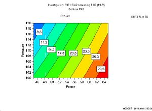
![[image:RIE1_SIO2_DOE1_Etch_rate.jpg|300x300px|thumb|left|Etch rate as a function of power and pressure at 70% CHF<sub>3</sub>. The etch rate decreases a little as a function of %CHF<sub>3</sub>. ]] | |||
|- | |||
|} | |||
|- | |||
|} | |||
<br clear="all" /> | |||
'''Selectivity to photoresist''' | |||
{| border="0" cellspacing="1" cellpadding="3" align="Left" | |||
! | |||
{| border="2" cellspacing="1" cellpadding="3" align="Left" | |||
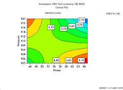
![[image:RIE1_SIO2_DOE1_Selectivitet_65.jpg|250x200px|thumb|Left|Selectivity as a function of power and pressure at 65% CHF<sub>3</sub>. ]] | |||
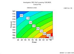
![[image:DOE1_SIO2_RIE1_Selectivitet_70.jpg|250x200px|thumb|Left|Selectivity as a function of power and pressure at 70% CHF<sub>3</sub>. ]] | |||
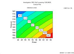
![[image:RIE1_SIO2_DOE1_Selectivity_75.jpg|250x200px|thumb|Left|Selectivity as a function of power and pressure at 75% CHF<sub>3</sub>. ]] | |||
|- | |||
|} | |||
|- | |||
|} | |||
<br clear="all" /> | |||
'''Etch profile angle''' <br\> | |||
The etch profile was also examined but there was not found any significant correlation between the profile angle and the process parameters. | |||
Latest revision as of 15:18, 6 February 2023
Feedback to this page: click here
This page is written by Berit Herstrøm @ DTU Nanolab (BGHE) if nothing else is stated
Both RIE's (RIE1 and RIE2) for silicon based etching has been decommissioned
RIE (Reactive Ion Etch) can be used for etching silicon oxide. The etch is anisotropic with vertical or angled sidewalls depending on the process recipe and the masking material and geometry. The SiO2 is etched by flour radicals assisted by ion bombardment.
The substrate:
Must be a wafer of 4" or below or small pieces, not higher than about 2mm. The system can be set up for 6", please ask 2 weeks in advance.
The silicon can be masked by these materials:
- Photoresist
- E-beam resist
- Silicon
- Silicon Nitride
- Aluminium
- Other metals if they cover less than 5% of the wafer area.
Most used recipes:
QC results
| Quality Controle (QC) for RIE2 - oxide etch | ||||||||||||||||||||
|
Resist as masking material:
| Recipe: | 1SiO2mre |
|---|---|
| Masking material | Photoresist |
| CF4 flow | 14 sccm |
| CHF3 flow | 26 sccm |
| Pressure | 100 mTorr |
| RF-power | 60 W |
| Expected results in RIE1 (has been decommissioned) | Expected results in RIE2 | |
|---|---|---|
| Etch rate in SiO2 |
~20-30 nm/min |
~20-30 nm/min |
| Etch rate in Si3N4 | ? | ? |
| Etch rate in P-Si (when used as mask) |
~30 nm/min |
~30 nm/min |
| Etch rate in Si
(etching down to Si) |
Expected <2 nm/min |
Expected <2 nm/min |
mre:mask resist
PolySilicon as masking material
| Recipe: | 1SiO2msi |
|---|---|
| Masking material | Silicon |
| CF4 flow | 8 sccm |
| CHF3 flow | 40 sccm |
| Pressure | 150 mTorr |
| RF-power | 150 W |
| Expected results in RIE1 (HAS BEEN DECOMMISSIONED) | Expected results in RIE2 | |
|---|---|---|
| Etch rate in SiO2 |
~70-80 nm/min |
~70-80 nm/min |
| Etch rate in Si3N4 | ? | ? |
| Etch rate in P-Si (when used as mask) |
~20-30 nm/min |
~20-30 nm/min |
| Etch rate in Si
(etching down to Si) |
? | ? |
| Images | Etches with p-Si as masking material |
msi:mask silicon
The recipe: 1SiO2bre (se below) can also be used with p-Si as masking material.
Burned resist as masking material (developed for waveguides by Haiyan Ou @DTU Photonics):
| Recipe: | 1SiO2mbr |
|---|---|
| Masking material | Burned resist (250oC 1h) |
| CHF3 flow | 84 sccm |
| Pressure | 60 mTorr |
| RF-power | 200 W |
| Expected results in RIE1 (HAS BEEN DECOMMISSIONED) | Expected results in RIE2 | |
|---|---|---|
| Etch rate in SiO2 |
~120 nm/min |
~120 nm/min |
| Etch rate burned resist |
? |
? |
| Etch rate in Si3N4 |
? |
? |
| Etch rate in P-Si (when used as mask) |
? nm/min |
? nm/min |
| Etch rate in Si
(etching down to Si) |
? |
? |
| Images |
Etches with p-Si as masking material Etches with burned resist as masking material |
Etches with burned resist as masking material |
mbr:mask burned resist
A survey of the parameter space using photoresist as masking material
A DOE has been performed. A short summery is given here: (in progress)
RIE1: RIE1 has been decommissioned but the results are probably similar on RIE2
A Design Of Experiment (DOE) has been performed. A screening experiment: full factorial with to levels: 9 different runs and 3 repetitions. Results from a screening experiment should be taken "with a gain of salt" meaning use it only as a rough guide line and test your recipe before use.
|
The Design of the experiment
|
Etch rate |
|---|
Selectivity to photoresist
|
|
|---|
Etch profile angle <br\> The etch profile was also examined but there was not found any significant correlation between the profile angle and the process parameters.


