Specific Process Knowledge/Characterization/Four-Point Probe: Difference between revisions
| (One intermediate revision by the same user not shown) | |||
| Line 1: | Line 1: | ||
'''Feedback to this page''': '''[mailto:labadviser@danchip.dtu.dk?Subject=Feed%20back%20from%20page%20http://labadviser.danchip.dtu.dk/index.php/Specific_Process_Knowledge/Characterization/4-Point_Probe click here]''' | '''Feedback to this page''': '''[mailto:labadviser@danchip.dtu.dk?Subject=Feed%20back%20from%20page%20http://labadviser.danchip.dtu.dk/index.php/Specific_Process_Knowledge/Characterization/4-Point_Probe click here]''' | ||
''This page is written by DTU Nanolab internal'' | |||
==Four-Point Probe== | ==Four-Point Probe== | ||
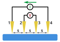
[[Image:Probe_diagram.PNG|thumb|200x200px|Probe diagram | [[Image:Probe_diagram.PNG|thumb|200x200px|Probe diagram. ''Drawing from https://www.ossila.com/pages/sheet-resistance-theory'']]The set-up of the four point probe is four the tungsten carbide electrodes/probes.The power source (DC) sends a current through the two outer electrodes. A digital voltage meter (DVM) measures the potential drop between the two inner electrodes. | ||
The sheet resistance can then be calculated using the equation below: | The sheet resistance can then be calculated using the equation below: | ||
Latest revision as of 13:03, 6 February 2023
Feedback to this page: click here
This page is written by DTU Nanolab internal
Four-Point Probe

The set-up of the four point probe is four the tungsten carbide electrodes/probes.The power source (DC) sends a current through the two outer electrodes. A digital voltage meter (DVM) measures the potential drop between the two inner electrodes.
The sheet resistance can then be calculated using the equation below:
This equation is only valid if: i) the material being tested is no thicker than 40% of the spacing between the probes, and ii) the lateral size of the sample is sufficiently large. If this is not the case, then geometric correction factors are needed to account for the size, shape, and thickness of the sample.
Bulk resistivity for wafers and films = sheet resistance x wafer thickness in cm (Unit ohm.cm)
Bulk resistivity for a semi-infinite volume = 2 x π x S x V/I where is S is the probe spacing in cm (Unit ohm.cm)
A sample is usually defined as a “semi-infinite volume” if it extends to infinity in all directions below a plane on which four probes are located.
Note:
Volume Resistivity = Volume Resistance = Bulk Resistivity = Bulk Resistance
Sheet Resistivity = Sheet Resistance = Surface Resistivity = Surface Resistance
Limits of the Measurement
1. The material must be capable of being probed, i.e. the probes must be able to make ohmic contact with the material e.g. Germanium, Silicon and metals. Materials such as Gallium Arsenide cannot normally be probed unless it is doped and measured with special measuring techniques such as that in the Four Dimensions Inc. GaAs probe.
2. Very low resistivity material e.g. aluminum, gold, platinum may require the maximum current from the current source to achieve a reading on the digital voltage display. Only very thin films from 10’s nm up to 1 micron thickness can be measured. Sample with expected sheet resistance less than 1 ohm/square may not possible to measure.
3. High resistivity material e.g. ion-implanted Silicon wafer, silicon on sapphire, can be measured using very low current (about 1uA or less) and trying to avoid a greater voltage indication than 200mV. Probably sheet resistance up to 107 ohms/square can be measured.
4. Low measurement result could be from electrical noise due to poor contact condition, thermally induced voltages, actinic effects, offset voltages produced by the devices in the current source etc.
There are two four point probes at DTU Nanolab. Four point probe from Jandel and Four-Point Probe from Veeco.
Four-Point Probe from Jandel

The Four point probe is manufactured by Jandel Engineering Limited and using Jandel probe head, a cylindrical probe type B: 1.00 mm spacing, 100 micron tip radius, 100g load linear is being use at Nanolab and the RM3000+ Test Unit which can supply constant current between 10nA and 99.99mA, and measure voltage from 0.01mV to 1250mV. The unit supplies a constant current and can display the resultant voltage, sheet resistance or volume resistivity depending which function has been chosen. For calculation of volume resistivity (for wafers or bulk samples) it is possible to input wafer thickness or probe spacing as required.
There is an Autorange feature: it will begin at 10 nA and increase the current by a factor of 10 until suitable level of measuring voltage is made and then it will stop and show the voltage or ohm/square on the display.
For sheet resistance measurements, the quoted range is 1 milliohm/square to 5x10⁸ ohms/square. Measurements outside this range are possible but with possible reduced accuracy. For volume (bulk) resistivity measurements, the quoted range is 1 milliohm.cm to 1x10⁶ ohm.cm. Measurements outside of this range may be possible but will depend on sample type e.g. whether the sample is a thin layer.
Multiposition Probe stand can measure on wafers up to 200mm diameter. The Θ movement clicks in four positions at 90 degrees and the linear movement in up to 10 positions giving repeat placement accuracy of +/- 1mm.
The user manual, technical information and contact information can be found in LabManager:
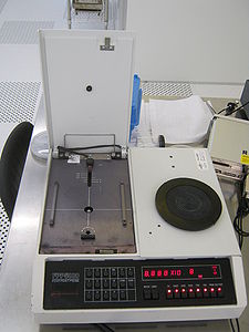
Four-Point Probe from Veeco
The Four-Point Probe is a Veeco FPP-5000. The main purpose is to measure film resistance and resistivity on a 4" or 6" wafer. And it can also be used to find film thickness as knowing film resistivity.

Only 4inch or 6inch wafers can be fitted in the system because a special holder is needed.
The user manual, technical information and contact information can be found in LabManager:
Overview of the performance of the Four-Point Probe at DTU Nanolab
| Four point probe - Jandel | Four point probe - Veeco | |
| Purpose | Measure voltage, sheet resistance or volume resistivity at varied current | Measure resistance, resistivity or film thickness(*) at 100uA |
| Unit | mV, ohm/square, ohm.cm(wafer), ohm.cm(volume) | ohm/square, ohm.cm, |
| Substrate | Small pieces up to 200mm wafer | Only 4inch or 6inch wafer |
(*) Knowing the resistivity
