Specific Process Knowledge/Etch/Etching of Silicon Oxide/SiO2 etch using AOE/Standard recipe with resist mask/Striation: Difference between revisions
| (25 intermediate revisions by the same user not shown) | |||
| Line 1: | Line 1: | ||
'''Feedback to this page''': '''[mailto:labadviser@ | '''Feedback to this page''': '''[mailto:labadviser@nanolab.dtu.dk?Subject=Feed%20back%20from%20page%20http://labadviser.nanolab.dtu.dk/index.php/Specific_Process_Knowledge/Etch/Etching_of_Silicon_Oxide/SiO2_etch_using_AOE/Standard_recipe_with_resist_mask/Striation click here]''' | ||
=Striation: Side wall roughness= | =Striation: Side wall roughness (This work was done in April 2016 by Berit Herstrøm, DTU Nanolab (bghe))= | ||
When etching silicon oxide rough sidewalls are most often seem. This effect is called striation, because it creates stripes along the etched profile. The literature gives several explanations for this. The two main courses seems to be: | When etching silicon oxide rough sidewalls are most often seem. This effect is called striation, because it creates stripes along the etched profile. The literature gives several explanations for this. The two main courses seems to be: | ||
| Line 10: | Line 10: | ||
#* Re-deposition of sputtered SiO2 | #* Re-deposition of sputtered SiO2 | ||
# damage of the resist mask coursed by plasma heating and/or interaction with the resist. This pattern change at the edge gets transferred to the oxide profile during the etch. | # damage of the resist mask coursed by plasma heating and/or interaction with the resist. This pattern change at the edge gets transferred to the oxide profile during the etch. | ||
#* Resist edge gets rough during etching due to plasma heating (out-gassing while the surface get UV hardened. This | #* Resist edge gets rough during etching due to plasma heating (out-gassing while the surface get UV hardened. This makes the resist crumple). | ||
#*The edge can maybe also get roughened due to sputtering. | #*The edge can maybe also get roughened due to sputtering. | ||
| Line 16: | Line 16: | ||
# First I characterized how our present three standard resists (AZ5214E, AZ nLof and AZ Mir) looked after an SiO2 etch in the AOE (recipe: SiO2_mres). The characterization was done by | # First I characterized how our present three standard resists (AZ5214E, AZ nLof and AZ Mir) looked after an SiO2 etch in the AOE (recipe: SiO2_mres). The characterization was done by | ||
#* SEM: to visually see the SiO2 sidewall roughness and how the resist looks after etch. This only gives a qualitative characterization. | #* SEM: to visually see the SiO2 sidewall roughness and how the resist looks after etch. This only gives a qualitative characterization. [[Specific_Process_Knowledge/Etch/Etching_of_Silicon_Oxide/SiO2_etch_using_AOE/Standard_recipe_with_resist_mask/Striation#Sidewall_roughness_and_resist_surface_after_AOE_etch_viewed_with_SEM_for_the_three_resists:_AZ5214E.2C_AZ_nLof_and_AZ_MIR |See HERE]] | ||
#* AFM: to get at quantitative value for the resist roughness after the etch. I have seem in the literature that this measure reflects the sidewall roughness of the resist. | #* AFM: to get at quantitative value for the resist roughness after the etch. I have seem in the literature that this measure reflects the sidewall roughness of the resist. [[Specific_Process_Knowledge/Etch/Etching_of_Silicon_Oxide/SiO2_etch_using_AOE/Standard_recipe_with_resist_mask/Striation#Roughness_of_the_resist_after_AOE_etch_measured_with_the_AFM_of_the_three_resists:_AZ5214E.2C_AZ_nLof_and_AZ_MIR |See HERE]] | ||
# Second we tried to toughen the resist by cross linking (by UV flood exposure after development) and heat treatment. Heat treatment at 110 degrees to effectuate the cross linking and heat treatment at 150 degrees to further out-gas and harden the resist. This was only | # Second we tried to toughen the resist by cross linking (by UV flood exposure after development) and heat treatment. Heat treatment at 110 degrees to effectuate the cross linking and heat treatment at 150 degrees to further out-gas and harden the resist. This was only done to AZ5214E and AZ nLof as AZ MIR? | ||
#*Results for the AZ nLof resist: [[Specific_Process_Knowledge/Etch/Etching_of_Silicon_Oxide/SiO2_etch_using_AOE/Standard_recipe_with_resist_mask/Striation#Sidewall_roughness.2Fresist_surface_roughness_effected_by_UV_curing_and_heat_treatment_of_nLof_resist |See HERE]]. | |||
#*Results for the AZ5214E [[Specific_Process_Knowledge/Etch/Etching_of_Silicon_Oxide/SiO2_etch_using_AOE/Standard_recipe_with_resist_mask/Striation#Sidewall_roughness.2Fresist_surface_roughness_effected_by_UV_curing_and_heat_treatment_of_AZ5214E_resist | See HERE]] | |||
<br clear="all"/> | <br clear="all"/> | ||
| Line 25: | Line 27: | ||
<gallery caption="Striation with different resists used" widths="300px" heights="250px" perrow="4"> | <gallery caption="Striation with different resists used" widths="300px" heights="250px" perrow="4"> | ||
Image:Az1_1_06.jpg| | Image:Az1_1_06.jpg|Az5214E resist, tilted 30 degrees. Resist is rough after etch and striation is seen on both the resist and the SiO2 | ||
Image:Az1_1_07.jpg| | Image:Az1_1_07.jpg|Az5214E resist, tilted 30 degrees. Resist is rough after etch and striation is seen on both the resist and the SiO2, bad resist work | ||
Image:Az1_1_10.jpg| | Image:Az1_1_10.jpg|Az5214E resist, tilted 30 degrees. Resist is rough after etch and striation is seen on both the resist and the SiO2 | ||
Image:az1_p1_31.jpg| | Image:az1_p1_31.jpg|Az5214E resist - profile after etch | ||
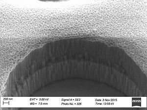
Image:Mir1_1_21.jpg|Mir resist | Image:Mir1_1_21.jpg|AZ Mir resist, tilted 30 degrees. Resist is rough after etch and striation is seen on the SiO2 but looks less severe on the resist, but maybe it is the SEM quality. | ||
Image:Mir1_1_18.jpg|Mir resist | Image:Mir1_1_18.jpg|AZ Mir resist, tilted 30 degrees. Resist is rough after etch and striation is seen. Bad resist work. | ||
Image:Mir1_1_24.jpg|Mir resist | Image:Mir1_1_24.jpg|AZ Mir resist, tilted 30 degrees. Resist is rough after etch and striation is seen on the SiO2 but looks less severe on the resist, but maybe it is the SEM quality | ||
Image:MIR1_00.jpg|Mir resist - profile after etch | Image:MIR1_00.jpg|AZ Mir resist - profile after etch | ||
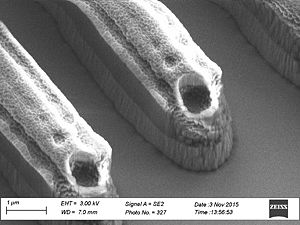
Image:nLof1_1_25.jpg|nLof | Image:nLof1_1_25.jpg|AZ nLof resist, tilted 30 degrees. Resist is rough after etch and striation is seen on both the resist and the SiO2. It looks less servere on the SiO2, this can be due to the fact that the resist profile on on a negative resist is negatively tappered. When etching the effect of a bad resist edge will smoothed in the bottom of the trench as the resist is thinned and thereby shrinked. But maybe it is the SEM quality. | ||
Image:nLof1_1_29.jpg|nLof | Image:nLof1_1_29.jpg|AZ nLof resist, tilted 30 degrees. Resist is rough after etch and striation is seen. Bad resist work probably narrowed the structures. | ||
Image:nLof1_1_27.jpg|nLof | Image:nLof1_1_27.jpg|AZ nLof resist, tilted 30 degrees. | ||
Image:nlof1_13.jpg|nLof resist - profile after etch | Image:nlof1_13.jpg|AZ nLof resist - profile after etch | ||
</gallery> | </gallery> | ||
==Roughness of the resist after AOE etch measured with the AFM of the three resists: AZ5214E, AZ nLof and AZ MIR== | ==Roughness of the resist after AOE etch measured with the AFM of the three resists: AZ5214E, AZ nLof and AZ MIR== | ||
<gallery widths="500px" heights="400px" perrow="3"> | <gallery caption="From these AFM measurements it looks like AZ nLof is least effected in roughness by the AOE etch, this could make sense because it is already cross linked" widths="500px" heights="400px" perrow="3"> | ||
Image:AZ1_3 after autoconfig.jpg| AZ5214E:Ra=3.98nm, Rmax=33,0nm | Image:AZ1_3 after autoconfig.jpg| AZ5214E:Ra=3.98nm, Rmax=33,0nm | ||
| Line 51: | Line 52: | ||
</gallery> | </gallery> | ||
==Sidewall roughness/resist surface roughness effected by UV curing and heat treatment of nLof resist== | |||
==Sidewall roughness/resist surface roughness effected by UV curing and heat treatment of nLof resist | |||
{| border="1" style="text-align: center; width: 320px; height: 200px;" | {| border="1" style="text-align: center; width: 320px; height: 200px;" | ||
|- | |- | ||
|colspan="6" style="text-align: center;" style="background: #000000; color: white;" | '''AOE etch with nLof resist with different treatments''' | |colspan="6" style="text-align: center;" style="background: #000000; color: white;" | '''AOE etch with nLof resist with different treatments'''´ | ||
|- | |||
|colspan="6" style="text-align: left;" style="background: #efefef;" |'''From AFM results from these tests it looks like it does not help to make further UV exposure to nLof resist but it does have some effect to heat it afterwards to 150dg. It has not been explored if this affects the CD (critical dimention). The SEM images does not confirm this improvement, maybe the image quality is not good enough.''' | |||
|- | |- | ||
!scope="row" | | !scope="row" | | ||
| Line 101: | Line 102: | ||
|} | |} | ||
==Sidewall roughness/resist surface roughness effected by UV curing and heat treatment of AZ5214E resist | ==Sidewall roughness/resist surface roughness effected by UV curing and heat treatment of AZ5214E resist== | ||
{| border="1" style="text-align: center; width: 320px; height: 200px;" | {| border="1" style="text-align: center; width: 320px; height: 200px;" | ||
|- | |- | ||
|colspan="6" style="text-align: center;" style="background: #000000; color: white;" | '''AOE etch with AZ5214E resist with different treatments''' | |colspan="6" style="text-align: center;" style="background: #000000; color: white;" | '''AOE etch with AZ5214E resist with different treatments''' | ||
|- | |||
|colspan="6" style="text-align: left;" style="background: #efefef;" |'''From AFM results from these tests it looks like it helps to make UV exposure and 110dg heat treatment to AZ5414E resist but it does not have convincing effect to heat it afterwards to 150dg. From the SEM images it is difficult to judge if the wall roughness is less. It does not look like a major difference.''' | |||
|- | |- | ||
!scope="row" | | !scope="row" | | ||
Latest revision as of 12:59, 3 February 2023
Feedback to this page: click here
Striation: Side wall roughness (This work was done in April 2016 by Berit Herstrøm, DTU Nanolab (bghe))
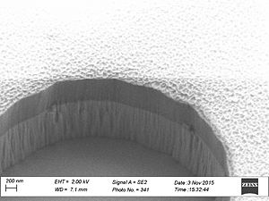
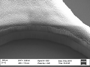
When etching silicon oxide rough sidewalls are most often seem. This effect is called striation, because it creates stripes along the etched profile. The literature gives several explanations for this. The two main courses seems to be:
- deposition on the sidewalls as the etch proceeds, coursing masking effects
- This can come from flour-carbon polymers from the plasma (some this this layer protects from striation)
- Re-deposition of sputtered SiO2
- damage of the resist mask coursed by plasma heating and/or interaction with the resist. This pattern change at the edge gets transferred to the oxide profile during the etch.
- Resist edge gets rough during etching due to plasma heating (out-gassing while the surface get UV hardened. This makes the resist crumple).
- The edge can maybe also get roughened due to sputtering.
This work is focused on trying to improve the resist to avoid the resist damage during etching. From a previous test it has been seen that pre baking the resist AZ1452e at 150 degrees for 5 min can prevent the crumpling of the resist, See results HERE. However this makes the resist flow so the edge profile will not remain vertical.
- First I characterized how our present three standard resists (AZ5214E, AZ nLof and AZ Mir) looked after an SiO2 etch in the AOE (recipe: SiO2_mres). The characterization was done by
- SEM: to visually see the SiO2 sidewall roughness and how the resist looks after etch. This only gives a qualitative characterization. See HERE
- AFM: to get at quantitative value for the resist roughness after the etch. I have seem in the literature that this measure reflects the sidewall roughness of the resist. See HERE
- Second we tried to toughen the resist by cross linking (by UV flood exposure after development) and heat treatment. Heat treatment at 110 degrees to effectuate the cross linking and heat treatment at 150 degrees to further out-gas and harden the resist. This was only done to AZ5214E and AZ nLof as AZ MIR?
Sidewall roughness and resist surface after AOE etch viewed with SEM for the three resists: AZ5214E, AZ nLof and AZ MIR
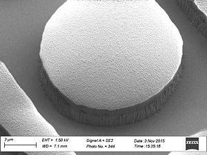
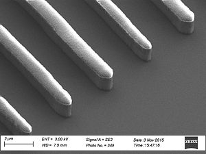
- Striation with different resists used
Az5214E resist, tilted 30 degrees. Resist is rough after etch and striation is seen on both the resist and the SiO2
Az5214E resist, tilted 30 degrees. Resist is rough after etch and striation is seen on both the resist and the SiO2, bad resist work
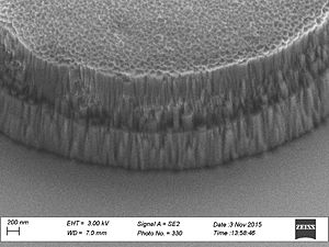
Az5214E resist, tilted 30 degrees. Resist is rough after etch and striation is seen on both the resist and the SiO2
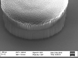
Az5214E resist - profile after etch
AZ Mir resist, tilted 30 degrees. Resist is rough after etch and striation is seen on the SiO2 but looks less severe on the resist, but maybe it is the SEM quality.

AZ Mir resist, tilted 30 degrees. Resist is rough after etch and striation is seen. Bad resist work.
AZ Mir resist, tilted 30 degrees. Resist is rough after etch and striation is seen on the SiO2 but looks less severe on the resist, but maybe it is the SEM quality
AZ Mir resist - profile after etch
AZ nLof resist, tilted 30 degrees. Resist is rough after etch and striation is seen on both the resist and the SiO2. It looks less servere on the SiO2, this can be due to the fact that the resist profile on on a negative resist is negatively tappered. When etching the effect of a bad resist edge will smoothed in the bottom of the trench as the resist is thinned and thereby shrinked. But maybe it is the SEM quality.
AZ nLof resist, tilted 30 degrees. Resist is rough after etch and striation is seen. Bad resist work probably narrowed the structures.
AZ nLof resist, tilted 30 degrees.
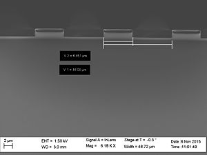
AZ nLof resist - profile after etch


Roughness of the resist after AOE etch measured with the AFM of the three resists: AZ5214E, AZ nLof and AZ MIR
- From these AFM measurements it looks like AZ nLof is least effected in roughness by the AOE etch, this could make sense because it is already cross linked
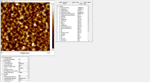
AZ5214E:Ra=3.98nm, Rmax=33,0nm
AZ MIR: Ra=4.55nm, Rmax=36.3nm
AZ nLof 2020: Ra=3.31nm, Rmax=28.0nm


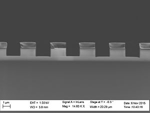
Sidewall roughness/resist surface roughness effected by UV curing and heat treatment of nLof resist
| AOE etch with nLof resist with different treatments´ | |||||
| From AFM results from these tests it looks like it does not help to make further UV exposure to nLof resist but it does have some effect to heat it afterwards to 150dg. It has not been explored if this affects the CD (critical dimention). The SEM images does not confirm this improvement, maybe the image quality is not good enough. | |||||
| 1 | 2 | 3 | 4 | 5 | |
|---|---|---|---|---|---|
| Treatment | No treatment before AOE etch | No treatment after 5min AOE etch | Flood-E 70s + 1min@110dg | 5min@150dg | Flood-E 70s + 60s@110dg + 5min@150dg |
| SEM image | 
|

|

|

|

|
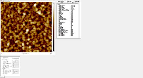
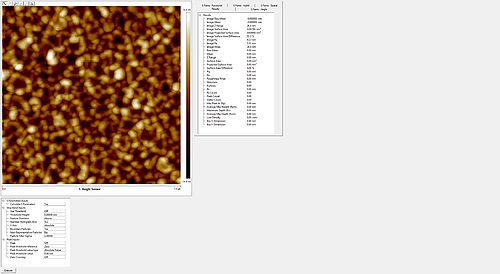
| AFM roughness scan | Ra=2.1nm Rmax=25.1nm 
|
Ra=3.31nm Rmax=28.0nm 
|
Ra=3.34nm Rmax=26.8nm 
|
Ra=2.45nm, Rmax=19.4nm 
|
Ra=2.52nm, Rmax=23.7nm 
|
| D | D1 | D2 | D3 | D4 | D5 |
Sidewall roughness/resist surface roughness effected by UV curing and heat treatment of AZ5214E resist
| AOE etch with AZ5214E resist with different treatments | |||||
| From AFM results from these tests it looks like it helps to make UV exposure and 110dg heat treatment to AZ5414E resist but it does not have convincing effect to heat it afterwards to 150dg. From the SEM images it is difficult to judge if the wall roughness is less. It does not look like a major difference. | |||||
| 1 | 2 | 3 | 4 | ||
|---|---|---|---|---|---|
| Treatment | No treatment before AOE etch | No treatment after 5min AOE etch | Flood-E 55s + 120s@110dg | Flood-E 55s + 120s@110dg + 5min@150dg | |
| SEM image | 
|

|

|

| |
| AFM roughness scan | Pre etch: cannot measure | Ra=4.40nm, Rmax=36.5nm 
|
Ra=3.68nm, Rmax=25.6nm 
|
Ra=3.57nm, Rmax=28.5nm 
| |
| D | D1 | D2 | D3 | D4 | |