Specific Process Knowledge/Etch/Etching of Bulk Glass/AOE etching of fused silica: Difference between revisions
| (44 intermediate revisions by 2 users not shown) | |||
| Line 1: | Line 1: | ||
'''Feedback to this page''': '''[mailto: | '''Feedback to this page''': '''[mailto:labadviser@nanolab.dtu.dk?Subject=Feed%20back%20from%20page%20http://labadviser.nanolab.dtu.dk/index.php/Specific_Process_Knowledge/Etch/Etching_of_Bulk_Glass/AOE_etching_of_fused_silica click here]''' | ||
==Comparison of masking materials and AOE processes etching fused silica== | ==Comparison of masking materials and AOE processes etching fused silica== | ||
{{CC-bghe2}} | |||
{|border="1" cellspacing="1" cellpadding="3" style="text-align:left;" | {|border="1" cellspacing="1" cellpadding="3" style="text-align:left;" | ||
|- | |- | ||
| Line 9: | Line 9: | ||
|-style="background:silver; color:black" | |-style="background:silver; color:black" | ||
! | ! | ||
!AZ resist mask | !AZ resist mask (Recipe name: SiO2_res) | ||
!PolySi mask | !PolySi mask (Recipe name: SiO2_psi) | ||
!Cr mask | !Cr mask (Recipe mane: SiO2_met) | ||
|- | |- | ||
|-style="background:LightGrey; color:black" | |||
|-style="background: | |||
!Generel description | !Generel description | ||
|Using a photoresist mask as etching mask is often convenient, since it takes less process steps to make than hard masks. The draw backs using resist as masking material in the AOE on glass is that glass does not transfer heat well and therefore the He cooling in the AOE does not work well on glass substrates. This makes the photoresist turn very hot during the etch and that might burn the resist. Resist also has low selectivity to glass so deep glass etch is not working well with photoresist as masking material. | |Using a photoresist mask as etching mask is often convenient, since it takes less process steps to make than hard masks. The draw backs using resist as masking material in the AOE on glass is that glass does not transfer heat well and therefore the He cooling in the AOE does not work well on glass substrates. This makes the photoresist turn very hot during the etch and that might burn the resist. Resist also has low selectivity to glass so deep glass etch is not working well with photoresist as masking material. | ||
|Using Poly Silicon as masking material in the AOE has the advantage over photoresist in the fact that the mask can stand a higher temperature. Then a recipe with higher etch can be used. It also as a higher selectivity so it is possible to etch deeper.The draw back might be higher line width reduction but this has not been expored yet. | |Using Poly Silicon as masking material in the AOE has the advantage over photoresist in the fact that the mask can stand a higher temperature. Then a recipe with higher etch can be used. It also as a higher selectivity so it is possible to etch deeper.The draw back might be higher line width reduction but this has not been expored yet. | ||
|This recipe with a Cr mask gives the highest etch rate, but the wafer uniformity is not so good. | |||
|-style="background:WhiteSmoke; color:black" | |||
!Substrate | |||
| | | | ||
*Fused silica 100mm | |||
| | | | ||
*Fused silica 100mm | |||
| | |||
*Fused silica 100mm | |||
|- | |- | ||
|-style="background:LightGrey; color:black" | |-style="background:LightGrey; color:black" | ||
| Line 34: | Line 37: | ||
*2µm | *2µm | ||
| | | | ||
*Cr | |||
*300nm | |||
Pattern defined in the ICP metal | |||
|- | |||
|-style="background:WhiteSmoke; color:black" | |-style="background:WhiteSmoke; color:black" | ||
|''Coil Power'' | |''Coil Power'' | ||
| Line 42: | Line 48: | ||
*1300 W | *1300 W | ||
| | | | ||
* | *1100W | ||
|-style="background:LightGrey; color:black" | |-style="background:LightGrey; color:black" | ||
|''Platen Power'' | |''Platen Power'' | ||
| Line 50: | Line 56: | ||
*500 W | *500 W | ||
| | | | ||
* | *180W | ||
|-style="background:WhiteSmoke; color:black" | |-style="background:WhiteSmoke; color:black" | ||
|''Platen temperature'' | |''Platen temperature'' | ||
| Line 58: | Line 64: | ||
*60<sup>o</sup>C | *60<sup>o</sup>C | ||
| | | | ||
* | *60<sup>o</sup>C | ||
|-style="background:LightGrey; color:black" | |-style="background:LightGrey; color:black" | ||
|''He flow'' | |''He flow'' | ||
| Line 66: | Line 72: | ||
*300 sccm | *300 sccm | ||
| | | | ||
* | *0 sccm | ||
|-style="background:WhiteSmoke; color:black" | |-style="background:WhiteSmoke; color:black" | ||
|''C<sub>4</sub>F<sub>8</sub> flow'' | |''C<sub>4</sub>F<sub>8</sub> flow'' | ||
| Line 74: | Line 80: | ||
*18 sccm | *18 sccm | ||
| | | | ||
* | *40 sccm | ||
|-style="background:LightGrey; color:black" | |-style="background:LightGrey; color:black" | ||
|''O<sub>2</sub> flow'' | |||
| | |||
*0 sccm | |||
| | |||
*0 sccm | |||
| | |||
*5 sccm | |||
|-style="background:WhiteSmoke; color:black" | |||
|''H<sub>2</sub> flow'' | |''H<sub>2</sub> flow'' | ||
| | | | ||
| Line 82: | Line 96: | ||
*0 sccm | *0 sccm | ||
| | | | ||
* | *0 sccm | ||
|-style="background: | |||
|-style="background:LightGrey; color:black" | |||
|''Pressure'' | |''Pressure'' | ||
| | | | ||
| Line 90: | Line 105: | ||
*4 mTorr | *4 mTorr | ||
| | | | ||
* | *6 mTorr | ||
|- | |- | ||
|-style="background: | |-style="background:WhiteSmoke; color:black" | ||
!Etch rate in fused silica | !Etch rate in fused silica | ||
| | | | ||
| Line 98: | Line 113: | ||
*173.5±0.5nm/min @40min etch (2013-03-13) (100nm Al on back side) | *173.5±0.5nm/min @40min etch (2013-03-13) (100nm Al on back side) | ||
*208nm/min @(5+5)min (2013-08-27) (no Al on back side, He pressure 6.8T) | *208nm/min @(5+5)min (2013-08-27) (no Al on back side, He pressure 6.8T) | ||
Reduced etch rate in long etch might be due to | ± refers to the variation over the wafer.<br> | ||
Reduced etch rate in long etch might be due to resist gone at the end. The polymer/resist left on the wafer after etch was less than 20nm and it looked burned. | |||
| | | | ||
*448.6±0.6nm/min @40min etch (2013-3-26) | *448.6±0.6nm/min @40min etch (2013-3-26) | ||
± refers to the variation over the wafer. | ± refers to the variation over the wafer. | ||
| | | | ||
* | *562nm/min±4.1nm/min @20min etch (2013-6-7) | ||
|- | |- | ||
|- | |- | ||
|-style="background: | |-style="background:LightGrey; color:black" | ||
!Selectivity to mask | !Selectivity to mask | ||
| | | | ||
| Line 115: | Line 130: | ||
| | | | ||
*~1:16 (2013-03-26) | *~1:16 (2013-03-26) | ||
| | |||
*~1:77 (2013-6-7) | |||
|- | |||
|-style="background:WhiteSmoke; color:black" | |||
!Linewidth reduction | |||
| | | | ||
* | * | ||
| | | | ||
*~4µm for this 17.8µm deep etch | |||
*~0.22µm/1µm etch depth | |||
| | |||
*~3µm for this 11.6µm deep etch | |||
*~0.26µm/1µm etch depth | |||
|- | |- | ||
|-style="background:LightGrey; color:black" | |-style="background:LightGrey; color:black" | ||
| Line 128: | Line 151: | ||
*100 mm wafer | *100 mm wafer | ||
| | | | ||
* | *100 mm wafer | ||
|- | |||
|-style="background:WhiteSmoke; color:black" | |||
!Images | |||
| | |||
| | |||
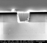
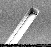
<gallery caption="vertical sidewalls" widths="300px" heights="200px" perrow="2"> | |||
image:AOE_fused_silica_m_polySi_n9_1.jpg|Etch profile viewed by SEM - Particulates are from the cleaving process | |||
image:AOE_fused_silica_m_polySi_n9_2.jpg|Etch profile viewed by SEM - Particulates are from the cleaving process | |||
image:AOE_fused_silica_m_polySi_n9_3.jpg|Etched lines viewed in a tilted angle by SEM - Particulates are from the cleaving process | |||
</gallery> | |||
| | |||
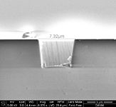
<gallery caption="Bowed sidewalls" widths="300px" heights="250px" perrow="2"> | |||
image:Glass-13 Cr mask 20130918 1.jpg|Etch profile viewed by SEM - Particulates are from the cleaving process | |||
image:Glass-13 Cr mask 20130918 2.jpg|Etch profile viewed by SEM - Particulates are from the cleaving process | |||
</gallery> | |||
|- | |- | ||
| Line 134: | Line 174: | ||
<br clear="all" /> | <br clear="all" /> | ||
==User results== | |||
===Done by Joachim Thomsen (student at Nanotech) October 2013=== | |||
The process flow was: | |||
*Fused silica wafers | |||
*Deposition of poly-Si on the wafers: LPCVD poly-Si furnace, recipe poly620, 1h30m: aprox. thickness 700nm | |||
*Adding AZ resist mask | |||
*Etching the poly-Si mask: AOE recipe "si_etch": 30s | |||
*Etching the fused silica: using AOE recipe "m_polysi": 11min10sec | |||
Results: | |||
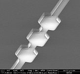
<gallery caption="5 µm channels in fused silica after AOE etch - the poly-Si mask is still on" widths="200px" heights="150px" perrow="4"> | |||
image:AOE fused silica Joachim Johansen 5my channel.jpg|Profile of 5µm channel | |||
image:AOE fused silica Joachim Johansen 5my channel after quartz etch 3 002.jpg|5 µm wide channel see from above (tilted) | |||
image:AOE fused silica Joachim Thomsen 5um channel after quartz etch 5 004.jpg|channel see from above (tilted) | |||
image:AOE fused silica Joachim Thomsen 5um channel after quartz etch 9 008.jpg|Profile of 5 µm channel | |||
</gallery> | |||
Latest revision as of 12:34, 3 February 2023
Feedback to this page: click here
Comparison of masking materials and AOE processes etching fused silica
Unless otherwise stated, all content in this section was done by Berit Herstrøm, DTU Nanolab
| AZ resist mask (Recipe name: SiO2_res) | PolySi mask (Recipe name: SiO2_psi) | Cr mask (Recipe mane: SiO2_met) | |
|---|---|---|---|
| Generel description | Using a photoresist mask as etching mask is often convenient, since it takes less process steps to make than hard masks. The draw backs using resist as masking material in the AOE on glass is that glass does not transfer heat well and therefore the He cooling in the AOE does not work well on glass substrates. This makes the photoresist turn very hot during the etch and that might burn the resist. Resist also has low selectivity to glass so deep glass etch is not working well with photoresist as masking material. | Using Poly Silicon as masking material in the AOE has the advantage over photoresist in the fact that the mask can stand a higher temperature. Then a recipe with higher etch can be used. It also as a higher selectivity so it is possible to etch deeper.The draw back might be higher line width reduction but this has not been expored yet. | This recipe with a Cr mask gives the highest etch rate, but the wafer uniformity is not so good. |
| Substrate |
|
|
|
| Mask material/thickness |
|
|
Pattern defined in the ICP metal |
| Coil Power |
|
|
|
| Platen Power |
|
|
|
| Platen temperature |
|
|
|
| He flow |
|
|
|
| C4F8 flow |
|
|
|
| O2 flow |
|
|
|
| H2 flow |
|
|
|
| Pressure |
|
|
|
| Etch rate in fused silica |
± refers to the variation over the wafer. |
± refers to the variation over the wafer. |
|
| Selectivity to mask |
|
|
|
| Linewidth reduction |
|
|
|
| Substrate size tried |
|
|
|
| Images |
|
|


User results
Done by Joachim Thomsen (student at Nanotech) October 2013
The process flow was:
- Fused silica wafers
- Deposition of poly-Si on the wafers: LPCVD poly-Si furnace, recipe poly620, 1h30m: aprox. thickness 700nm
- Adding AZ resist mask
- Etching the poly-Si mask: AOE recipe "si_etch": 30s
- Etching the fused silica: using AOE recipe "m_polysi": 11min10sec
Results:
- 5 µm channels in fused silica after AOE etch - the poly-Si mask is still on
Profile of 5µm channel
5 µm wide channel see from above (tilted)
channel see from above (tilted)
Profile of 5 µm channel


