Specific Process Knowledge/Etch/Etching of Silicon/Si etch using ASE: Difference between revisions
| (46 intermediate revisions by 5 users not shown) | |||
| Line 1: | Line 1: | ||
'''Feedback to this page''': '''[mailto:labadviser@nanolab.dtu.dk?Subject=Feed%20back%20from%20page%20http://labadviser.nanolab.dtu.dk/index.php/Specific_Process_Knowledge/Etch/Etching_of_Silicon/Si_etch_using_ASE click here]''' | |||
==The Bosch process: Etching of silicon== | ==The Bosch process: Etching of silicon== | ||
| Line 5: | Line 8: | ||
In the case of the silicon etching on the ASE, an etch phase with SF<sub>6</sub> and O<sub>2</sub> alternates with a passivation phase with C<sub>4</sub>F<sub>8</sub>. | In the case of the silicon etching on the ASE, an etch phase with SF<sub>6</sub> and O<sub>2</sub> alternates with a passivation phase with C<sub>4</sub>F<sub>8</sub>. | ||
== | == Quality control procedure on the ASE== | ||
Two recipes have been optimized for the ASE. Their specification is on a 10 % etch load wafer with trenches. | Two recipes have been optimized for the ASE. Their specification is on a 10 % etch load wafer with trenches. | ||
* '''Shallolr''': The shallow etch process will etch a 2 | * '''Shallolr''': The shallow etch process will etch a 2 µm opening down to make a 20 µm trench. | ||
* '''Deepetch''': The deep etch process will etch a 50 | * '''Deepetch''': The deep etch process will etch a 50 µm opening down to make a 300 µm trench. | ||
The standardization procedure on the ASE covers these two etches. | The standardization procedure on the ASE covers these two etches. | ||
== | {| border="1" cellspacing="2" cellpadding="2" colspan="3" | ||
|bgcolor="#98FB98" |'''Quality Control (QC) for ASE''' | |||
|- | |||
| | |||
*[http://labmanager.dtu.dk/d4Show.php?id=1607&mach=105 The QC procedure for ASE] | |||
*[http://labmanager.dtu.dk/view_binary.php?fileId=1751 The newest QC data for ASE] | |||
{| {{table}} | |||
| align="center" | | |||
{| border="1" cellspacing="1" cellpadding="2" align="center" style="width:400px" | |||
! QC Recipe: | |||
! colspan="4" |Shallolr (2 µm trench) | |||
|- | |- | ||
! colspan="2" align="center"| Common parameters | ! colspan="2" align="center"| Common parameters | ||
| Line 46: | Line 52: | ||
! Process time | ! Process time | ||
| 5:56 mins | | 5:56 mins | ||
! C<sub>4</sub>F<sub> | ! C<sub>4</sub>F<sub>8</sub> Flow | ||
| 0 sccm | | 0 sccm | ||
| 120 sccm | | 120 sccm | ||
| Line 69: | Line 75: | ||
|} | |} | ||
| align="center" valign="top"| | |||
{| border="2" cellspacing="1" cellpadding="2" align="center" style="width:400px" | |||
!QC limits | |||
! ASE | |||
|- | |||
|Etch rate in Si | |||
|3 - 4 µm/min | |||
|- | |||
|Non-uniformity | |||
| 5 % | |||
|- | |||
|} | |||
|- | |||
|} | |||
{| {{table}} | |||
| align="center" | | |||
{| border="1" cellspacing="1" cellpadding="2" align="center" style="width:400px" | |||
! QC Recipe: | |||
| | ! colspan="4" | Deepetch (50 µm trench) | ||
|- | |- | ||
! colspan="2" align="center"| Common parameters | ! colspan="2" align="center"| Common parameters | ||
| Line 110: | Line 121: | ||
! Process time | ! Process time | ||
| 54:10 mins | | 54:10 mins | ||
! C<sub>4</sub>F<sub> | ! C<sub>4</sub>F<sub>8</sub> Flow | ||
| 0 sccm | | 0 sccm | ||
| 120 sccm | | 120 sccm | ||
| Line 132: | Line 143: | ||
| 5 s | | 5 s | ||
|} | |} | ||
| align="center" valign="top"| | |||
{| border="2" cellspacing="1" cellpadding="2" align="center" style="width:400px" | |||
!QC limits | |||
! ASE | |||
|- | |||
|Etch rate in Si | |||
| 4 - 6 µm/min | |||
|- | |||
|Non-uniformity | |||
| 5 % | |||
|- | |||
|} | |||
|- | |||
|} | |||
|} | |||
== Recipes on the ASE == | |||
=== Shallolr === | |||
The shallolr recipe is designed to etch features (with sizes above 1 µm) in silicon down to a depth that ranges from a few microns to some 50 microns. (If you need to etch deeper use Deepetch or more shallow, see Nanoetches.) It is specified to etch a 2 µm wide trench down to a depth of 20 µm on a wafer that has a global/local etch opening density of 10%. | |||
The recipe is given above. | |||
The process runs for 31 cycles (5:56 mins). The fact that it's Bosch process is clear from the scallops on the sidewalls - one should be able to count 31 of them. | |||
<gallery caption="Standardization images of the shallolr recipe" widths="300px" heights="300px" perrow="2"> | |||
Image:jmlshal070921 pos1 2mu_09.jpg|The profile of a 2 µm trench | |||
image:jmlshal070921 pos1 50mu_08.jpg|The profile of a 50 µm trench | |||
</gallery> | |||
The process is designed to reach 20 µm down in a 2 µm trench but as is clear from the image of the corresponding 50 µm trench, this one is etched deeper. The reason is the so called Aspect Ratio Dependent Etching or ARDE: See below. | |||
=== Deepetch === | |||
The deepetch recipe is designed to etch features (with sizes 2 µm) in silicon down to a depth that ranges from some 50 microns to hundreds of microns. (If you need to etch less, use shallow or Nanoetches.) It is specified to etch a 50 µm wide trench down to a depth of 300 µm on a wafer that has a global/local etch density of 10%. | |||
<gallery caption="Standardization images of the deepetch recipe" widths="300px" heights="300px" perrow="2"> | <gallery caption="Standardization images of the deepetch recipe" widths="300px" heights="300px" perrow="2"> | ||
Image:jmldeep071101 pos1 2mu_010.jpg|The profile of a 2 | Image:jmldeep071101 pos1 2mu_010.jpg|The profile of a 2 µm trench | ||
image:jmldeep071101 pos5 50mu_013.jpg|The profile of a 50 | image:jmldeep071101 pos5 50mu_013.jpg|The profile of a 50 µm trench | ||
</gallery> | </gallery> | ||
As is clear from the two images ARDE also plays a role in this case: The 2 | As is clear from the two images ARDE also plays a role in this case: The 2 µm trench (widened to about 5-6 µm because of undercut/underetching) is only etched 150 µm. | ||
===Iso=== | |||
The recipe Iso is the same recipe as Deepetch but without the passivation steps. <br> | |||
It has been tested once by Filip Sandborg-Olsen @nanotech. <br> | |||
He etched with 100% load for 10 min. He got an etch rate of 5.51µm/min | |||
== Process development == | == Process development == | ||
===Etch of nano sized structures=== | ===Etch of nano sized structures=== | ||
{{Template:Author-bghe-thissection}} | |||
*See pxnano2 and comparison with nanotech on the Pegasus: [[Specific Process Knowledge/Etch/DRIE-Pegasus/nanoetch/nano142-pxnano2]] | |||
Older work: | |||
Three different examples of etch are shown here. The masking material was zep520A (80 nm). | Three different examples of etch are shown here. The masking material was zep520A (80 nm). | ||
| Line 217: | Line 272: | ||
| | | | ||
|- | |- | ||
|} | |||
<br clear="all"/> | |||
==Etching Si without back side cooling== | |||
{{Template:Author-bghe-thissection}} | |||
Etching in an ICP as the ASE without backside cooling normally results in heating up the sample to more than 100 degrees Celsius. This can be problematic especially when using resist as a masking material. <br> | |||
There can be many reasons for not applying cooling to the sample. Among these are samples that need to be processed on a carrier due to sensitive backsides, sticky backsides or structures on the backside, small samples, membranes that can break, bowing wafers or something else. <br> | |||
To meet these needs we have developed a silicon etch in the RIE mode where the coil power is not being used. The coil creates a high density plasma and that has a higher plasma temperature than a low density plasma created by the platen power in RIE mode. <br> | |||
This recipe is intended to only for low etch depths that are not very critical with regards to eg. the sidewall profile. For deep etching of silicon you will need to use the bosch process and the coil power. | |||
''' Recipe name in the ASE: "1si_rie1" ''' | |||
{| border="1" cellspacing="1" cellpadding="1" align="left" | |||
! Wafer ID | |||
! '''Resist before etch''' | |||
! '''Platen power''' | |||
! '''Pressure''' | |||
! '''Flow rate SF6''' | |||
! '''Flow rate O2''' | |||
! '''Flow rate Ar''' | |||
! width="20"| '''T''' | |||
! '''Process time''' | |||
! '''Comment''' | |||
! width="205"|'''Results''' | |||
! '''CD change''' | |||
! '''Profile angles''' | |||
! width="150"|'''Etch rate in Si''' | |||
! '''Etch rate in resist''' | |||
! '''Selectivity (resist:Si)''' | |||
! '''Etch rate in SiO2''' | |||
|- | |||
|- | |||
|-style="background:white; color:black" | |||
|ASE RIE9 | |||
|<!-- '''Resist before etch''' --> 3750nm | |||
|<!--'''Platen power'''--> 100W | |||
|<!--'''Pressure'''--> 80mTorr | |||
|<!--'''Flow rate CF4'''--> 40sccm | |||
|<!--'''Flow rate O2'''--> 27sccm | |||
|<!--'''Flow rate Ar'''-->0 | |||
|<!--'''T'''--> 20 | |||
|<!--'''Process time'''--> 30min | |||
|<!--'''Comment'''--> HBC off, resist not burned. Microscope images! | |||
|<!--'''Results'''-->[[File:ASE RIE9 d.jpg|200px]][[File:ASE RIE9 f.jpg|200px]] | |||
|<!--'''CD change (mask 55% trench) after s007467 is it <50% after barc etch'''<br> | |||
trench opening as a fraction of pitch--> | |||
. | |||
|<!--'''Profile angles'''--> | |||
. | |||
|<!--'''Etch rate in Si'''--> | |||
443.3 nm/min | |||
|<!--'''Etch rate in resist'''--> | |||
91.7 nm/min | |||
|<!--'''Selectivity (resist:Si)'''--> | |||
1:4.8 | |||
|<!--'''Etch rate in SiO2'''--> | |||
32 nm/min | |||
SRN:60 nm/min | |||
|- | |||
|-style="background:white; color:black" | |||
|ASE RIE8 | |||
|<!-- '''Resist before etch''' --> 3750nm | |||
|<!--'''Platen power'''--> 100W | |||
|<!--'''Pressure'''--> 80mTorr | |||
|<!--'''Flow rate CF4'''--> 40sccm | |||
|<!--'''Flow rate O2'''--> 27sccm | |||
|<!--'''Flow rate Ar'''-->0 | |||
|<!--'''T'''--> 20 | |||
|<!--'''Process time'''--> 4min | |||
|<!--'''Comment'''--> HBC off Microscope images! | |||
|<!--'''Results'''-->[[File:ASE RIE8 b.jpg|200px]][[File:ASE RIE8 c.jpg|200px]] | |||
|<!--'''CD change (mask 55% trench) after s007467 is it <50% after barc etch'''<br> | |||
trench opening as a fraction of pitch--> | |||
. | |||
|<!--'''Profile angles'''--> | |||
. | |||
|<!--'''Etch rate in Si'''--> | |||
440 nm/min | |||
|<!--'''Etch rate in resist'''--> | |||
nm/min | |||
|<!--'''Selectivity (resist:Si)'''--> | |||
|<!--'''Etch rate in Si'''--> | |||
? | |||
|} | |} | ||
Latest revision as of 09:38, 3 February 2023
Feedback to this page: click here
The Bosch process: Etching of silicon
The Bosch process uses alternation between an etch cycle and a passivation cycle. Introducing a passivation step in an etch process is very beneficial for the control of the angle of the sidewalls in the etch process because it allows us to cover them with a protective layer that suppresses the isotropic etching. Combined with the high plasma density in the ICP chamber, the excellent sidewall control enables us to etch high aspect ratio structures in silicon with very high etch rates.
In the case of the silicon etching on the ASE, an etch phase with SF6 and O2 alternates with a passivation phase with C4F8.
Quality control procedure on the ASE
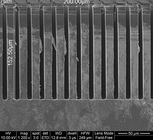
Two recipes have been optimized for the ASE. Their specification is on a 10 % etch load wafer with trenches.
- Shallolr: The shallow etch process will etch a 2 µm opening down to make a 20 µm trench.
- Deepetch: The deep etch process will etch a 50 µm opening down to make a 300 µm trench.
The standardization procedure on the ASE covers these two etches.
| Quality Control (QC) for ASE | ||||||||||||||||||||||||||||||||||||||||||||||||||||||||||||||||||||||||||||||||||||||||||||||||||||||||||
| ||||||||||||||||||||||||||||||||||||||||||||||||||||||||||||||||||||||||||||||||||||||||||||||||||||||||||
Recipes on the ASE
Shallolr
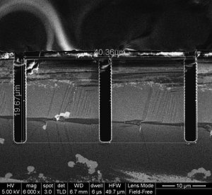
The shallolr recipe is designed to etch features (with sizes above 1 µm) in silicon down to a depth that ranges from a few microns to some 50 microns. (If you need to etch deeper use Deepetch or more shallow, see Nanoetches.) It is specified to etch a 2 µm wide trench down to a depth of 20 µm on a wafer that has a global/local etch opening density of 10%.
The recipe is given above.
The process runs for 31 cycles (5:56 mins). The fact that it's Bosch process is clear from the scallops on the sidewalls - one should be able to count 31 of them.
- Standardization images of the shallolr recipe
-
 The profile of a 2 µm trench
 -
 The profile of a 50 µm trench


The process is designed to reach 20 µm down in a 2 µm trench but as is clear from the image of the corresponding 50 µm trench, this one is etched deeper. The reason is the so called Aspect Ratio Dependent Etching or ARDE: See below.
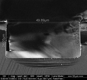
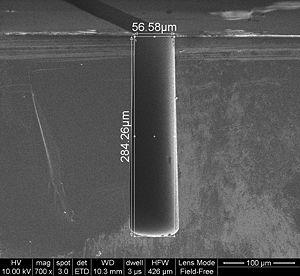
Deepetch
The deepetch recipe is designed to etch features (with sizes 2 µm) in silicon down to a depth that ranges from some 50 microns to hundreds of microns. (If you need to etch less, use shallow or Nanoetches.) It is specified to etch a 50 µm wide trench down to a depth of 300 µm on a wafer that has a global/local etch density of 10%.
- Standardization images of the deepetch recipe
-
 The profile of a 2 µm trench
 -
 The profile of a 50 µm trench


As is clear from the two images ARDE also plays a role in this case: The 2 µm trench (widened to about 5-6 µm because of undercut/underetching) is only etched 150 µm.
Iso
The recipe Iso is the same recipe as Deepetch but without the passivation steps.
It has been tested once by Filip Sandborg-Olsen @nanotech.
He etched with 100% load for 10 min. He got an etch rate of 5.51µm/min
Process development
Etch of nano sized structures
The content on this section was created by Berit Herstrøm, DTU Nanolab
- See pxnano2 and comparison with nanotech on the Pegasus: Specific Process Knowledge/Etch/DRIE-Pegasus/nanoetch/nano142-pxnano2
Older work: Three different examples of etch are shown here. The masking material was zep520A (80 nm).
| Vertical sidewalls | Low ARDE | Positive tappered side walls |
|---|---|---|

|

|

|

|

|

|
|
Etch cycle
Dep. Cycle
Results:
|
Etch cycle
Dep. Cycle
Results:
|
Etch cycle
Dep. Cycle
Results:
|
Etching Si without back side cooling
The content on this section was created by Berit Herstrøm, DTU Nanolab
Etching in an ICP as the ASE without backside cooling normally results in heating up the sample to more than 100 degrees Celsius. This can be problematic especially when using resist as a masking material.
There can be many reasons for not applying cooling to the sample. Among these are samples that need to be processed on a carrier due to sensitive backsides, sticky backsides or structures on the backside, small samples, membranes that can break, bowing wafers or something else.
To meet these needs we have developed a silicon etch in the RIE mode where the coil power is not being used. The coil creates a high density plasma and that has a higher plasma temperature than a low density plasma created by the platen power in RIE mode.
This recipe is intended to only for low etch depths that are not very critical with regards to eg. the sidewall profile. For deep etching of silicon you will need to use the bosch process and the coil power.
Recipe name in the ASE: "1si_rie1"
| Wafer ID | Resist before etch | Platen power | Pressure | Flow rate SF6 | Flow rate O2 | Flow rate Ar | T | Process time | Comment | Results | CD change | Profile angles | Etch rate in Si | Etch rate in resist | Selectivity (resist:Si) | Etch rate in SiO2 |
|---|---|---|---|---|---|---|---|---|---|---|---|---|---|---|---|---|
| ASE RIE9 | 3750nm | 100W | 80mTorr | 40sccm | 27sccm | 0 | 20 | 30min | HBC off, resist not burned. Microscope images! |  
|
. |
. |
443.3 nm/min |
91.7 nm/min |
1:4.8 |
32 nm/min SRN:60 nm/min
|
| ASE RIE8 | 3750nm | 100W | 80mTorr | 40sccm | 27sccm | 0 | 20 | 4min | HBC off Microscope images! |  
|
. |
. |
440 nm/min |
nm/min |
?
|